Film deposition apparatus and film deposition method

a film deposition apparatus and film technology, applied in chemical vapor deposition coating, coating, metallic material coating process, etc., can solve the problems of insufficient room in which the substrate is transferred, inability to achieve in-plane uniformity of the process, and inability to achieve uniform oxidization of high dielectric constant material adsorbed on the substrate in a sufficiently uniform manner. , to achieve the effect of solving the problem of high in-plane uniformity of the film thickness and excellent film quality

Active Publication Date: 2010-11-04
TOKYO ELECTRON LTD
View PDF90 Cites 310 Cited by
  • Summary
  • Abstract
  • Description
  • Claims
  • Application Information

AI Technical Summary

Benefits of technology

[0011]The present invention has been made in view of the above circumstances, so as to effectively solve these problems. The object of the present invention is to provide a film deposition ...

Problems solved by technology

Thus, there is a possibility that the high dielectric constant material adsorbed on the substrate might not be oxidized in a sufficiently uniform manner.
However, when the substrate is brought excessively close to the showerhead, there is not left enough room in which the substrate is transferred between an external transfer mechanism and a stage on which the substrate is to be placed.
This inhibits the in-plane uniformity of the process.
However, when the entire process container is heated to such a high temperature, a grease of a drive system for moving the stage upward and downward, a grease of another drive system fo...

Method used


Image

  • Film deposition apparatus and film deposition method
  • Film deposition apparatus and film deposition method
  • Film deposition apparatus and film deposition method

Examples


Embodiment Construction

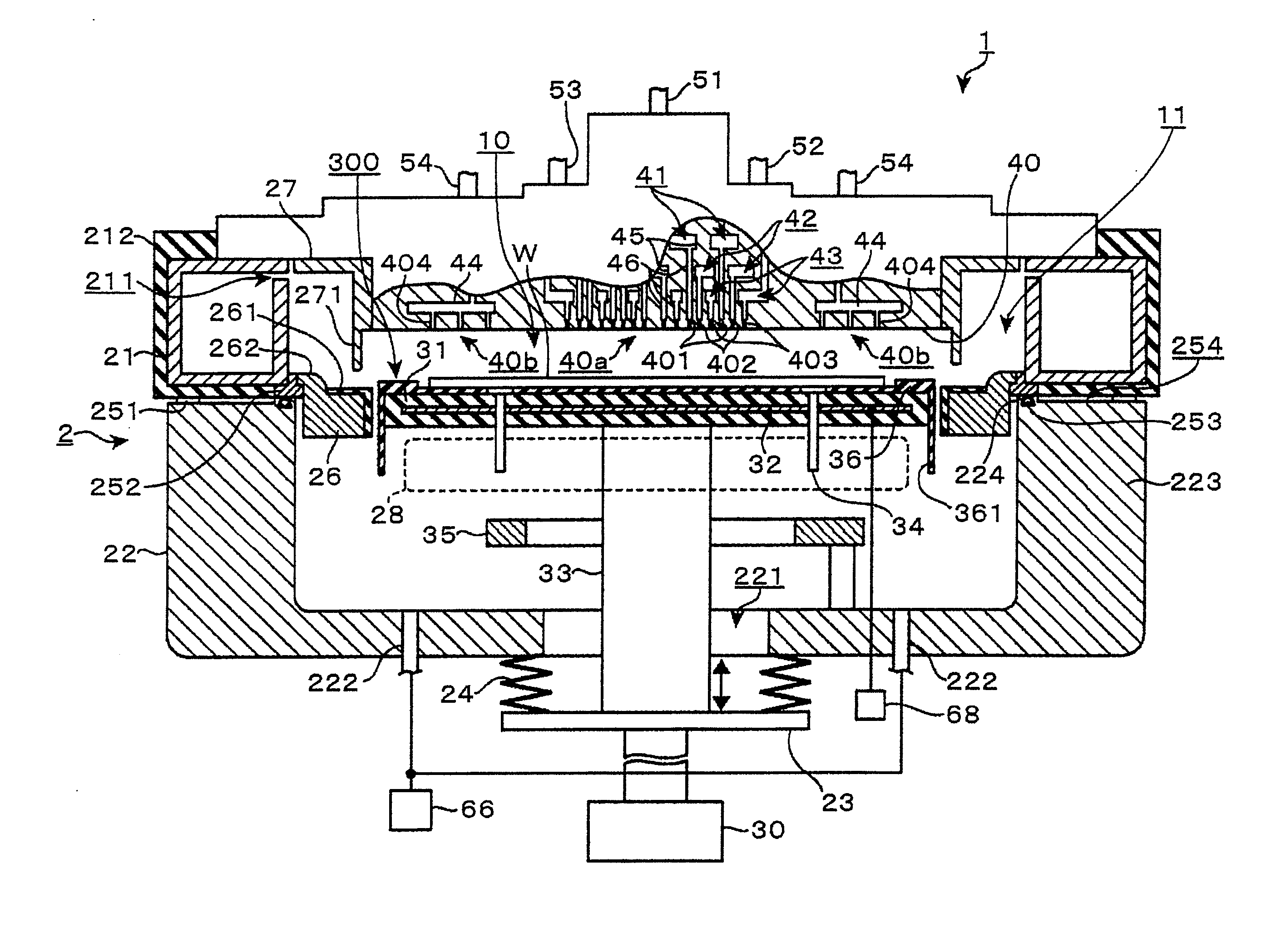
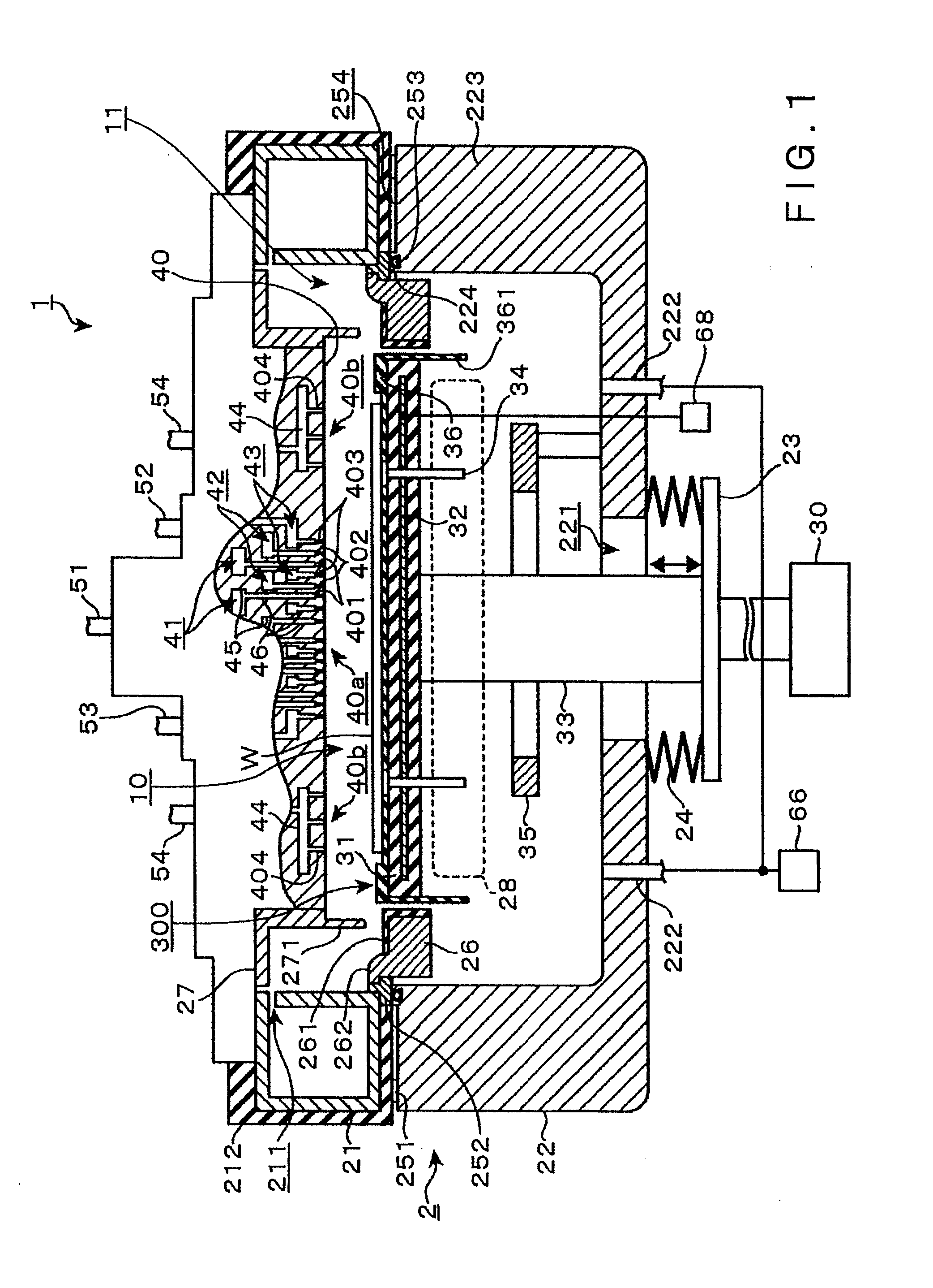
[0038]A structure of a film deposition apparatus in one embodiment of the present invention will be described herebelow with reference to FIGS. 1 to 4. In the film deposition apparatus 1 in this embodiment, for example, a material gas containing strontium (Sr) (hereinafter referred to as “Sr material”) and a material gas containing titanium (Ti) (hereinafter referred to as “Ti material”) are used as a first process gas, and an ozone gas as a reaction gas is used as a second process gas. The film deposition apparatus 1 reacts these process gases with each other by an ALD process, whereby a film made of strontium titanate (SrTiO3 (hereinafter abbreviated to “STO”)), which is a high dielectric constant material, is deposited on a surface of a wafer as a substrate.

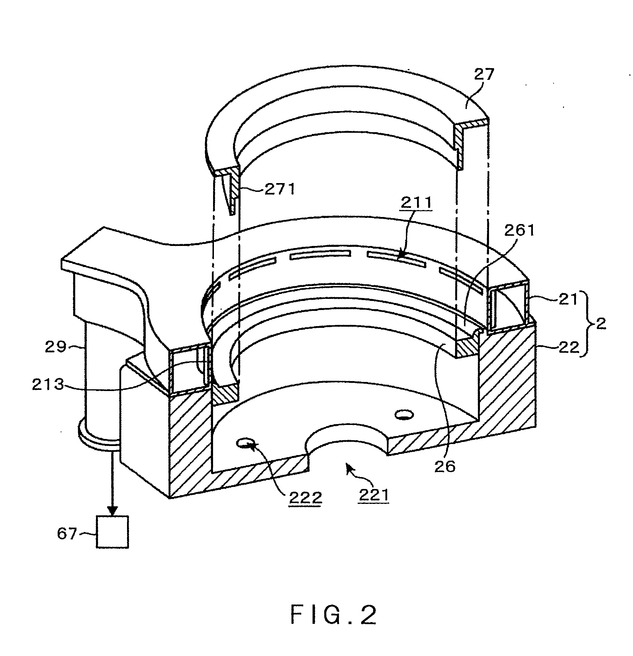
[0039]As shown in the longitudinal sectional view of FIG. 1, the film deposition apparatus 1 includes: a process container 2 forming a vacuum container; a stage 31 disposed in the process container 2, the stage 31 constituting...


PUM

PropertyMeasurementUnit
Temperatureaaaaaaaaaa
Electrical conductanceaaaaaaaaaa
Shapeaaaaaaaaaa

Abstract

The present invention is a film deposition apparatus configured to deposit a film on a substrate that has been loaded into a vacuum container via a transfer opening and placed on a table in the vacuum container, by supplying a process gas to the substrate from a process-gas supply part opposed to the table under a vacuum atmosphere, while heating a table surface of the table, the film deposition apparatus comprising: an elevating mechanism configured to vertically move the table between a process position at which the substrate is subjected to a film deposition process, and a transfer position at which the substrate is transferred to and from an external transfer mechanism that has entered from the transfer opening; a surrounding part configured to surround the table with a gap therebetween, when the table is located at the process position, so that the surrounding part and the table divide an inside of the vacuum container into an upper space, which is located above the table, and a lower space, which is located below the table; a vacuum exhaust conduit in communication with the upper space, through which a process atmosphere in the upper space is discharged to create a vacuum in the upper space; a heating unit configured to heat a gas contact region ranging from the upper space to the vacuum exhaust conduit, to a temperature higher than a temperature allowing adhesion of reactant; and a heat insulation part disposed between the heating unit and a lower part of the vacuum container surrounding the lower space.

Description

FIELD OF THE INVENTION[0001]The present invention relates to a technique for supplying a process gas to a substrate under vacuum atmosphere, so as to deposit, on the substrate, a film of a reaction product of the process gas.BACKGROUND ART[0002]As a film deposition method in a semiconductor manufacturing process, there has been known a method for depositing a film on a substrate, which makes, under vacuum atmosphere, a semiconductor wafer (hereinafter referred to as “wafer”), which is a substrate, adsorb a first process gas (material gas) on its surface, then switches a gas to be supplied from the first process gas to a second process gas (reaction gas) so as to form one or more atomic layers and molecular layers by the reaction of the first and second gases, and repeats this cycle plural times so as to stack these layers. This film deposition method, which is referred to as, e.g., an ALD (Atomic Layer Deposition) method or an MLD (Molecular Layer Deposition) method, can precisely c...

Claims


Application Information

Patent Timeline
IPC IPC(8): C23C16/44C23C16/46C23C16/52C23C16/458
CPCC23C16/409C23C16/44C23C16/4412C23C16/45565C23C16/4557H01L21/31691H01L21/02186H01L21/02197H01L21/0228H01L21/3141C23C16/45574
Inventor TAKAGI, TOSHIO
Owner TOKYO ELECTRON LTD
Why Eureka
Try Eureka