Nanocrystalline indium tin oxide sensors and arrays

Active Publication Date: 2010-11-04
NORTH FLORIDA UNIV OF
View PDF11 Cites 4 Cited by
  • Summary
  • Abstract
  • Description
  • Claims
  • Application Information

AI Technical Summary

Benefits of technology

[0012]In another aspect of the invention, the common electrode terminal and the plurality of discrete electrode terminals are each operably coupled to a device configured to monitor electrical resistance across each ITO film strip over time. The plurality of spaced apart ITO film strips is configured to experience a determined change in resistance in a determined amount of time after exposure to a gaseous chemical warfare agent. The plurality of sensors forms an array.
[0013]In yet another aspect of the invention a meth

Problems solved by technology

Particularly problematic for conventional sensors are the requirements for response time and sensitivity in ambient conditions.

Method used


Image

  • Nanocrystalline indium tin oxide sensors and arrays
  • Nanocrystalline indium tin oxide sensors and arrays
  • Nanocrystalline indium tin oxide sensors and arrays

Examples


Embodiment Construction

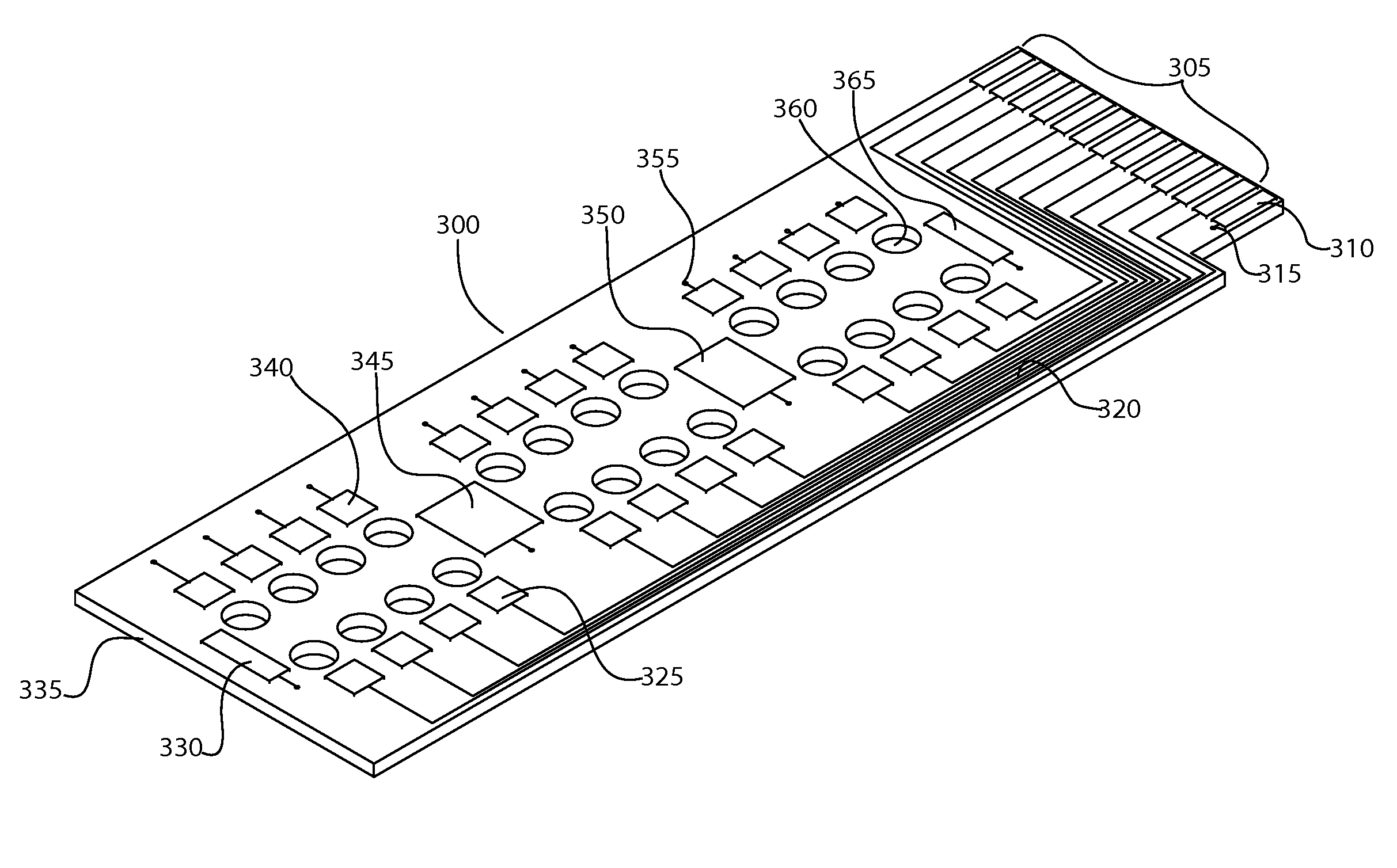
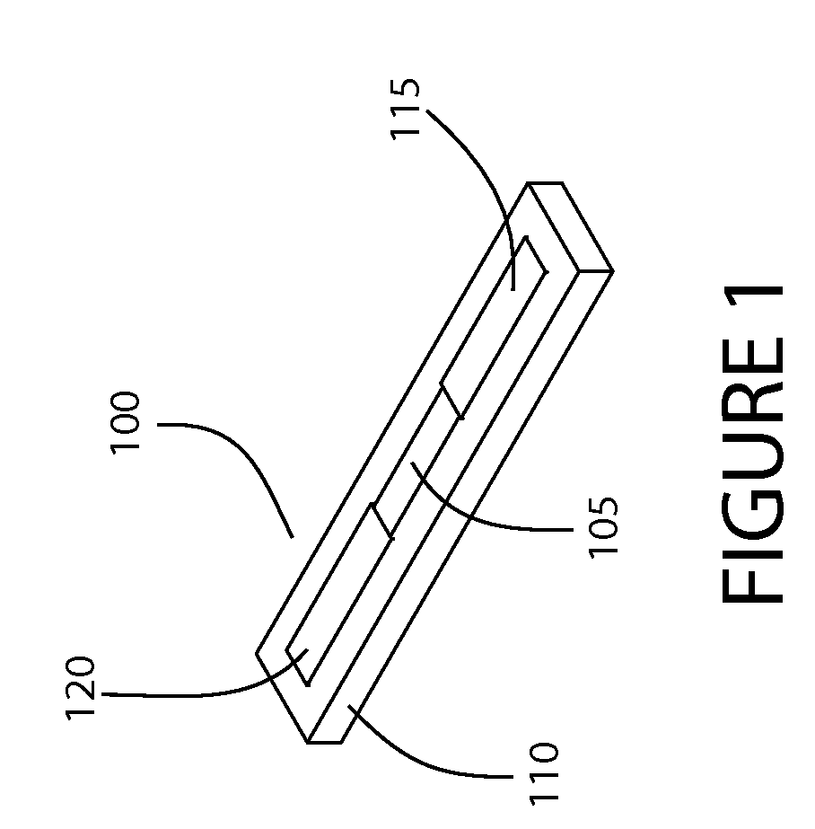
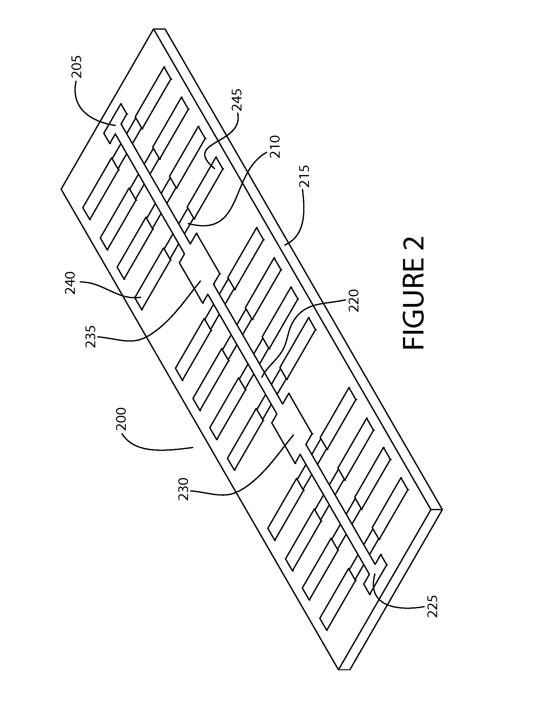
[0037]Referring to the Figures, in which like parts are indicated with the same reference numerals, various views of an exemplary sensor and a sensor array according to principles of the invention are shown. In general, an exemplary sensor according to principles of the invention comprises a nanocrystalline indium tin oxide (ITO, or tin-doped indium oxide) thin film applied to a substrate. The indium tin oxide film comprises a mixture of indium(III) oxide (In2O3) and tin(IV) oxide (SnO2), by way of example and not limitation 90% In2O3 and 10% SnO2 by weight. The substrate is an electrical insulator that is compatible with the process of forming the ITO thin film. By way of example and not limitation, glass, alumina Al2O3, silicon, silicon dioxide SiO2 or another compatible material may be utilized as the substrate. A pair of electrodes is conductively coupled to the film. The electrodes are configured for coupling to an electrical measurement device, such as an ohmmeter. Electrical ...


PUM


Abstract

A sensor for sensing gaseous chemicals includes a substrate, a variable resistance nanocrystalline ITO thin film formed on the substrate, and electrodes electrically coupled to the thin film. A sensor array assembly includes a sensor slide and a perforated interface circuit. The interface circuit abuts and electrically couples the sensor slide. The sensor slide includes several spaced apart ITO film strips formed on a slide substrate. A common electrode is electrically coupled to a common portion of each ITO film strip providing an electrically conductive path across the common portions of each of the plurality of spaced apart ITO film strips. A discrete electrode is electrically coupled to a discrete portion of each ITO film strip. The interface circuit is configured to abut and electrically couple to the sensor slide. A conductive discrete electrode pad electrically couples each of the plurality of discrete electrodes of the sensor slide to discrete terminals on the interface circuit. A conductive common electrode pad is associated with and electrically couples the common electrode of the sensor slide to a common electrode on the interface circuit. Apertures in the interface circuit expose the thin film to the environment. Resistance changes in a detectible manner upon exposure to sensible chemicals at ambient temperature, such as 1,2,2-Trimethylpropyl methylphosphonofluoridate (soman, GD), O-Ethyl S-(2-isopropylaminoethyl) methylphosphonothiolate (VX), distilled bis(2-chloroethyl) sulfide (mustard, HD), carbonyl chloride, Phosgene (CG) and cyanogen chloride (CK), ozone, carbon monoxide, carbon dioxide, acetylene, propane, ammonia, sulfur dioxide, ethanol, methanol, volatile organic compounds and industrial toxic chemicals.

Description

GOVERNMENT LICENSE RIGHTS[0001]The U.S. Government has a paid-up license in this invention and the right in limited circumstances to require the patent owner to license others on reasonable terms as provided for by the terms of DOD W911 SR-04-C-0072, awarded by the United States Army.FIELD OF THE INVENTION[0002]This invention generally relates to detection of chemical warfare agents, and, more particularly, to portable sensors for detecting a wide range of chemical warfare agents rapidly in ambient conditions.BACKGROUND[0003]As chemical warfare agents pose an ever increasing risk, an urgent need exists for reliable sensors. Ideally, a sensor would be portable and operate in ambient conditions to reliably detect a wide variety of chemical warfare agents (CWA) with exceptional sensitivity, selectivity and response time. In addition, the resulting system must be rugged, cost effective and of simple design, such that it may readily be deployed in any environmental setting. Particularly ...

Claims


Application Information

Patent Timeline
IPC IPC(8): G01N27/00G01N27/12G01N27/04
CPCG01N27/125G01N33/0039G01N33/004G01N33/0047G01N33/0054G01N33/0057Y02A50/20
Inventor PATEL, NIRMALKUMAR G.
Owner NORTH FLORIDA UNIV OF
Why Eureka
Try Eureka