

Light emitting diode with bonded semiconductor wavelength converter
- Summary
- Abstract
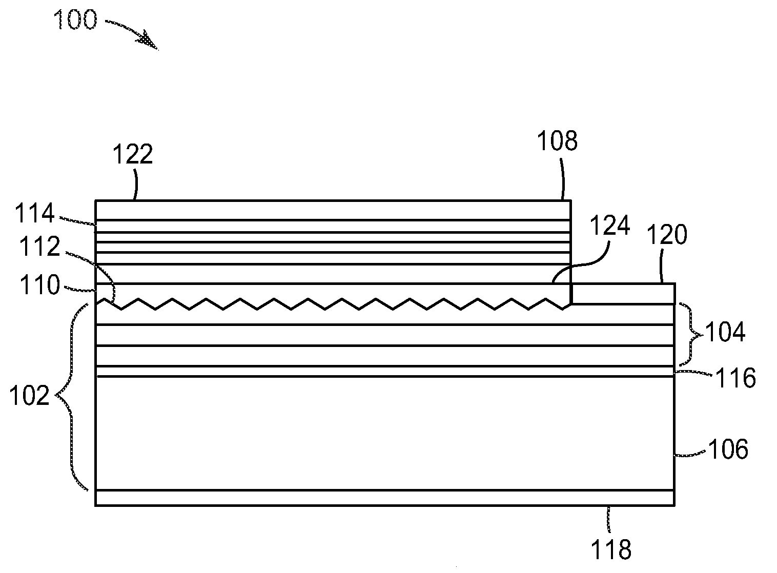
- Description
- Claims
- Application Information
AI Technical Summary
Benefits of technology
Problems solved by technology
Method used
Image

Examples
example 1
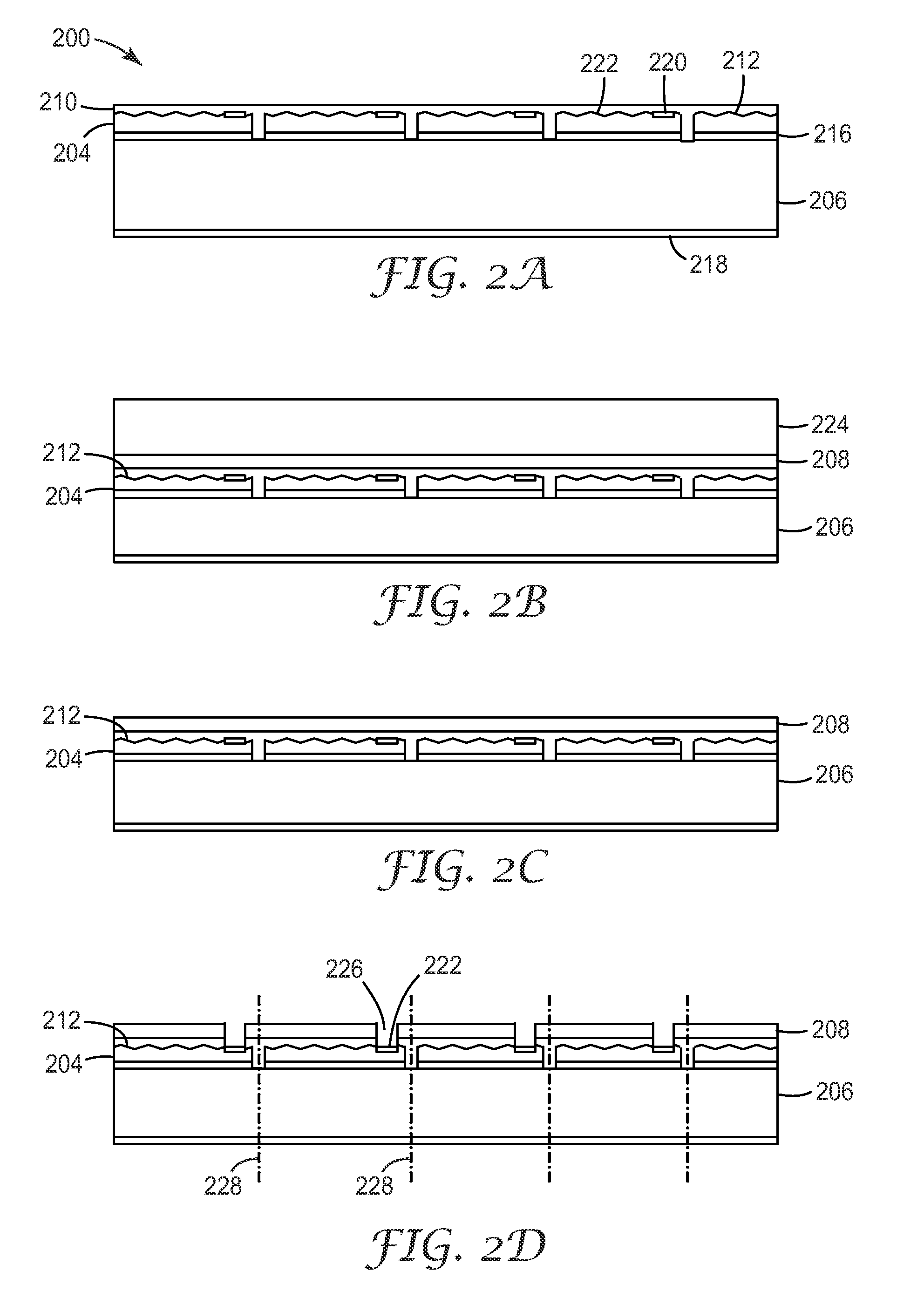
Metal-Bonded LED with Textured Surface
[0043]A wavelength converted LED was produced using a process like that illustrated in FIGS. 2A-2D. The LED wafer 200 was purchased from Epistar Corp., Hsinchu, Taiwan. The wafer 200 had epitaxial AlGaInN LED layers 204 bonded to a silicon substrate 206. As received, the n-type nitride on the upper side of the LED wafer was provided with 1 mm square mesas 222. In addition, the surface was roughened so that some portions had a textured surface 212. Other portions were metallized with gold Au traces to spread the current and to provide pads for wire bonding. The backside of the silicon substrate 206 was metallized with a gold-based layer 218 to provide the p-type contact.
[0044]A multilayer, quantum well semiconductor converter 208 was initially prepared on an InP substrate using molecular beam epitaxy (MBE). A GaInAs buffer layer was first grown by MBE on the InP substrate to prepare the surface for II-VI growth. The wafer was then moved through a...
example 2
Modeled Effect of the Textured Surface Versus a Flat Surface
[0057]A wavelength converted LED having different textured surfaces was modeled using TracePro 4.1 optical modeling software. The LED was modeled as a 1 mm×1 mm×0.01 mm block of GaN. The LED was assumed to be embedded in a hemisphere of encapsulant. The underside of the LED, i.e. the lower side of the LED substrate, was assumed to be provided with a silver reflector having a reflectivity of 88%. A bonding layer, having a thickness of 2 μm and having the same refractive index as the encapsulant, separated the emitting surface of the LED and the semiconductor wavelength converter layer. The converter layer was assumed to have a flat surface on both its input and output sides. The parameters of the model are summarized in Table I below.
TABLE IParameters in Used in Efficiency ModelingThicknessRefractiveAbsorption / Element(□m)IndexpassLED102.39 3% @ 460 nmBonding layer21.410%Wavelength converter22.5893% @ 460 nmlayerEncapsulant8 ...
PUM
 Abstract
Description
Claims
Application Information