Method and apparatus for suppressing noise caused by parasitic inductance and/or resistance in an electronic circuit or system

Active Publication Date: 2010-11-11
CITY UNIVERSITY OF HONG KONG
View PDF8 Cites 10 Cited by
  • Summary
  • Abstract
  • Description
  • Claims
  • Application Information

AI Technical Summary

Benefits of technology

[0035]In accordance with another main aspect of the invention, there is provided a method of reducing a parasitic effect in an electronic circuit. The method comprises determining a value of a parallel parasitic effect associated with a capacitor in the electronic circuit, sensing a voltage signal across the capacitor, determining from the sensed voltage signal and the value of the parallel parasitic effect a parasitic voltage associated with the capacitor, and adding a voltage source in series with the capacitor, the voltage source being adapted to deliver a compensating voltage of generally equal magnitude but generally opposit

Problems solved by technology

The increasing sophistication of electronic circuits and systems presents unique challenges for circuit designers.
However, the trend is hindered by the possible generation of undesirable effects, such as ringing and resonance, due to parasitic effects associated with the components, the physical orientation of the components, and/or the layout of components, devices and/or conductive tracks on printed circuit boards within an electronic circuit or system.
These parasitic elements degrade the high-frequency performance of the entire electronic circuit or system.
There are many electronic circuit or system designs where paras

Method used


Image

  • Method and apparatus for suppressing noise caused by parasitic inductance and/or resistance in an electronic circuit or system
  • Method and apparatus for suppressing noise caused by parasitic inductance and/or resistance in an electronic circuit or system
  • Method and apparatus for suppressing noise caused by parasitic inductance and/or resistance in an electronic circuit or system

Examples


Embodiment Construction

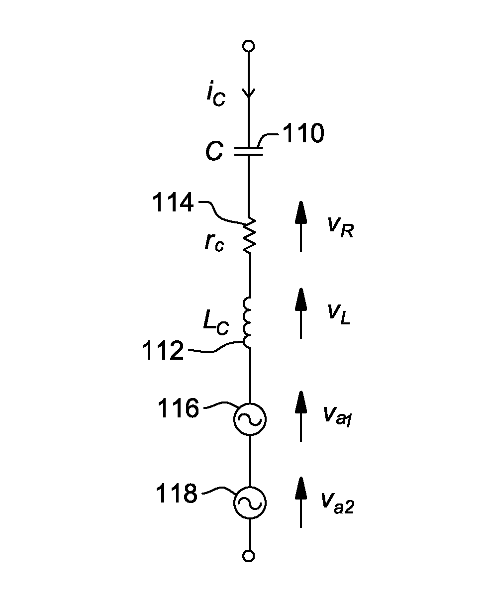
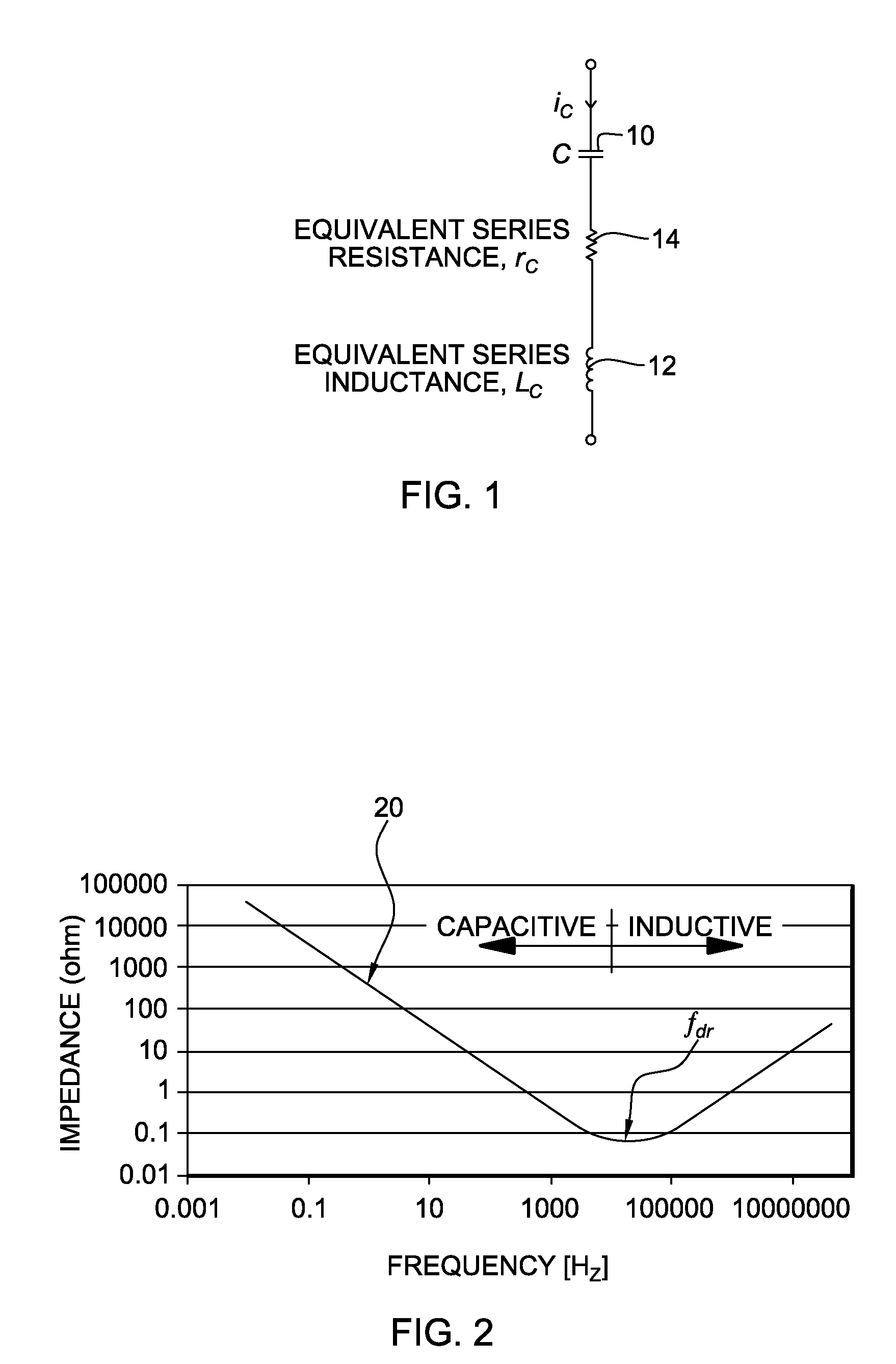
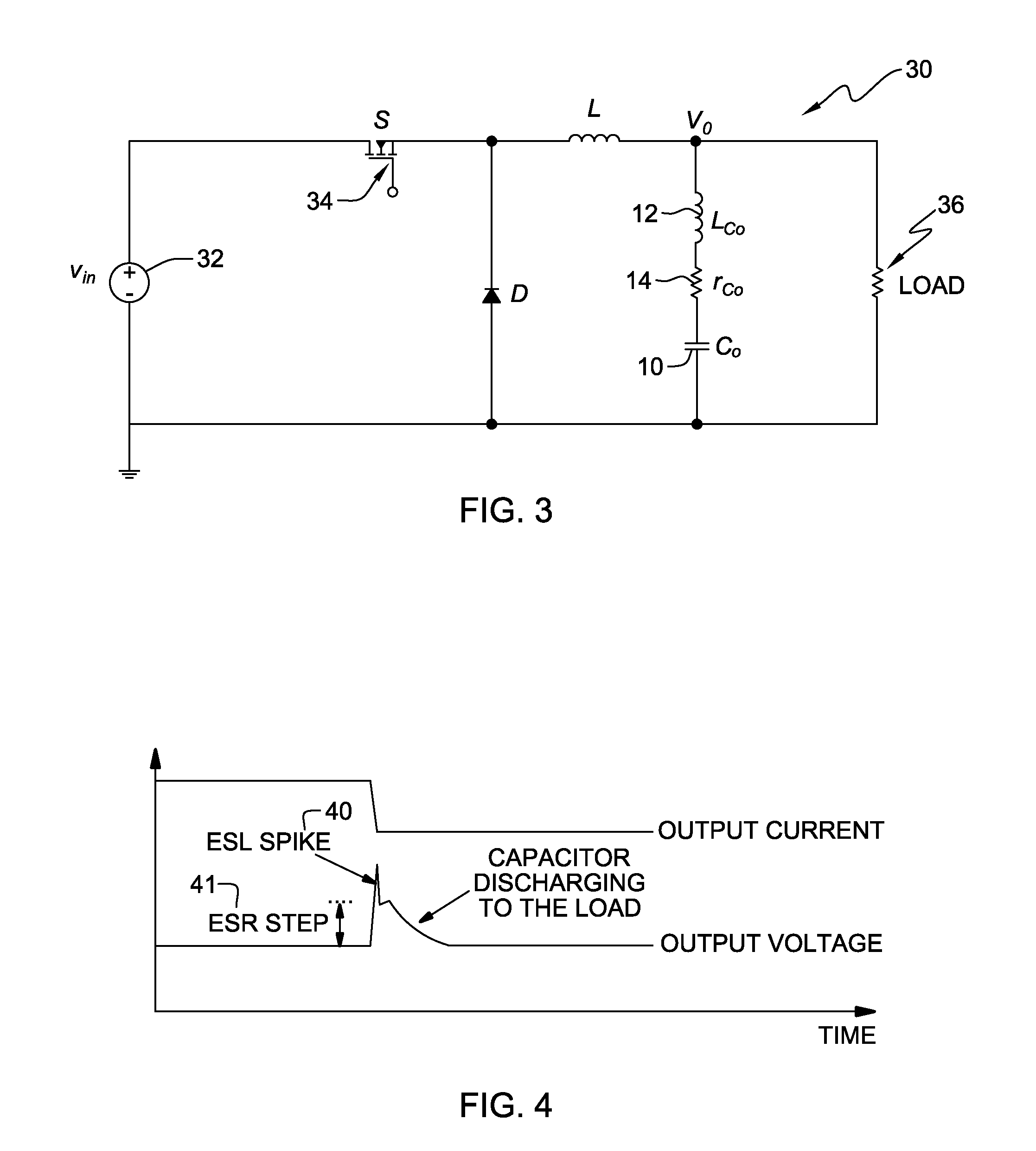
[0057]The present invention provides a method and system for reducing a parasitic effect in an electronic circuit or system. The method comprises: identifying a part of the electronic circuit or system that exhibits capacitance. This can be achieved through testing the circuit or system using known techniques. Alternatively, identification may merely comprise a recognition that a particular component such as a capacitor is designed to exhibit capacitance and that said level of capacitance is a designed feature of said component. A skilled person will be familiar with the many methods of identifying parts of a circuit or system or components of a circuit or system that exhibit some degree of capacitance. The method also comprises determining a value of a series parasitic effect associated with said part of the electronic circuit or system that exhibits capacitance. There are a wide range of methods for measuring parasitic inductance and again one skilled in the art will be familiar w...


PUM


Abstract

Reducing, suppressing or canceling series parasitic inductance and/or resistive effects that affect the frequency response of components, elements and/or circuits in an electronic circuit or system that exhibit capacitance is disclosed. Noise generated by series parasitic inductance and/or parasitic resistance of the components, the physical orientation of the components, and/or the layout of components, devices and/or conductive tracks (board traces) on printed circuit boards within an electronic circuit or system is reduced, suppressed or canceled. The reduction, suppression or cancellation is achieved by adding a voltage source in series with a part or component of the electronic circuit or system that exhibits capacitance, the current source being adapted to deliver a compensating voltage of roughly equal magnitude and roughly opposite phase to parasitic voltage associated with the part or component.

Description

CROSS-REFERENCE TO RELATED APPLICATIONS [0001]This application contains subject matter which is related to the subject matter of the following applications, each of which is assigned to the same assignee as this application and filed on the same day as this application. Each of the below listed applications is hereby incorporated herein by reference in its entirety:[0002]patent application Ser. No. 12 / 435,941, by CHUNG et al., entitled “METHOD AND APPARATUS FOR SUPPRESSING NOISE CAUSED BY PARASITIC CAPACITANCE AND / OR RESISTANCE IN AN ELECTRONIC CIRCUIT OR SYSTEM” (Attorney Docket No. 2055.097); and[0003]patent application Ser. No. 12 / 435,979, by CHUNG et al., entitled “AN OUTPUT COMPENSATOR FOR A REGULATOR” (Attorney Docket No. 2055.099).FIELD OF THE INVENTION[0004]The present invention relates generally to components, elements and / or circuits for reducing or suppressing parasitic inductance and / or resistive effects that affect the frequency response of the components, elements and / ...

Claims


Application Information

Patent Timeline
IPC IPC(8): G05F5/00
CPCH02M3/155H02M1/44
Inventor CHUNG, HENRY SHU HUNGYAN, WAI TO
Owner CITY UNIVERSITY OF HONG KONG
Why Eureka
Try Eureka