
Method for manufacturing epitaxial silicon wafer

a manufacturing method and silicon wafer technology, applied in the direction of crystal growth process, polycrystalline material growth, after-treatment details, etc., can solve the problems of reduced productivity, reduced productivity, and inability to completely treat the pits formed on the front surface of silicon wafers, so as to improve the micro-roughness (surface roughness) of the front surface of the wafer, without reducing productivity, and enhance the flatness of the wafer

Inactive Publication Date: 2010-11-18
SUMCO CORP
View PDF6 Cites 10 Cited by
  • Summary
  • Abstract
  • Description
  • Claims
  • Application Information

AI Technical Summary

Benefits of technology

The present invention provides a method of manufacturing an epitaxial silicon wafer that improves wafer flatness and reduces micro-roughness of the front surface without reducing productivity. The method includes chamfering the external peripheral surface of a sliced silicon wafer, flattening the front and rear surfaces of the wafer, etching the surfaces, and performing a gas-phase HF treatment on the front surface of the wafer. The method also allows for the removal of silicon oxide film from the internal surfaces of pits on the front surface of the wafer. The epitaxial film grown on the wafer is flat and smooth, and the method results in improved productivity and reduced micro-roughness of the front surface.

Problems solved by technology

Thus, a desired treatment cannot be completely performed on the pits formed on the front surface of the silicon wafer.
Consequently, productivity is not reduced, although the reduction in productivity is a problem of the conventional method of manufacturing epitaxial silicon wafers that includes an increased number of processes of polishing the wafer front surface (two times of front surface polishing before and after epitaxial growth).

Method used


Image

  • Method for manufacturing epitaxial silicon wafer
  • Method for manufacturing epitaxial silicon wafer
  • Method for manufacturing epitaxial silicon wafer

Examples


first embodiment

[0041]A method of manufacturing an epitaxial silicon wafer according to the first embodiment of the present invention is specifically explained. In the present embodiment, an epitaxial silicon wafer is produced in which an epitaxial film is grown on a front surface of a silicon wafer. The silicon wafer has a thickness of 725 μm and a diameter of 200 mm; and an axis direction of a main front surface is . The silicon wafer is a p-type wafer.

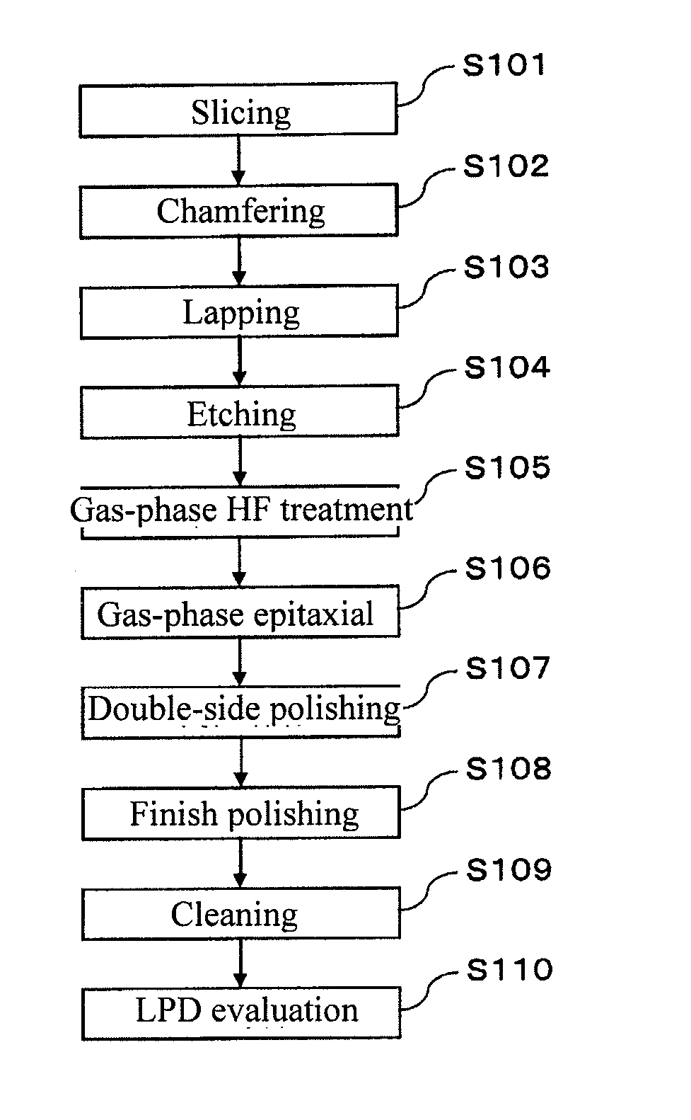
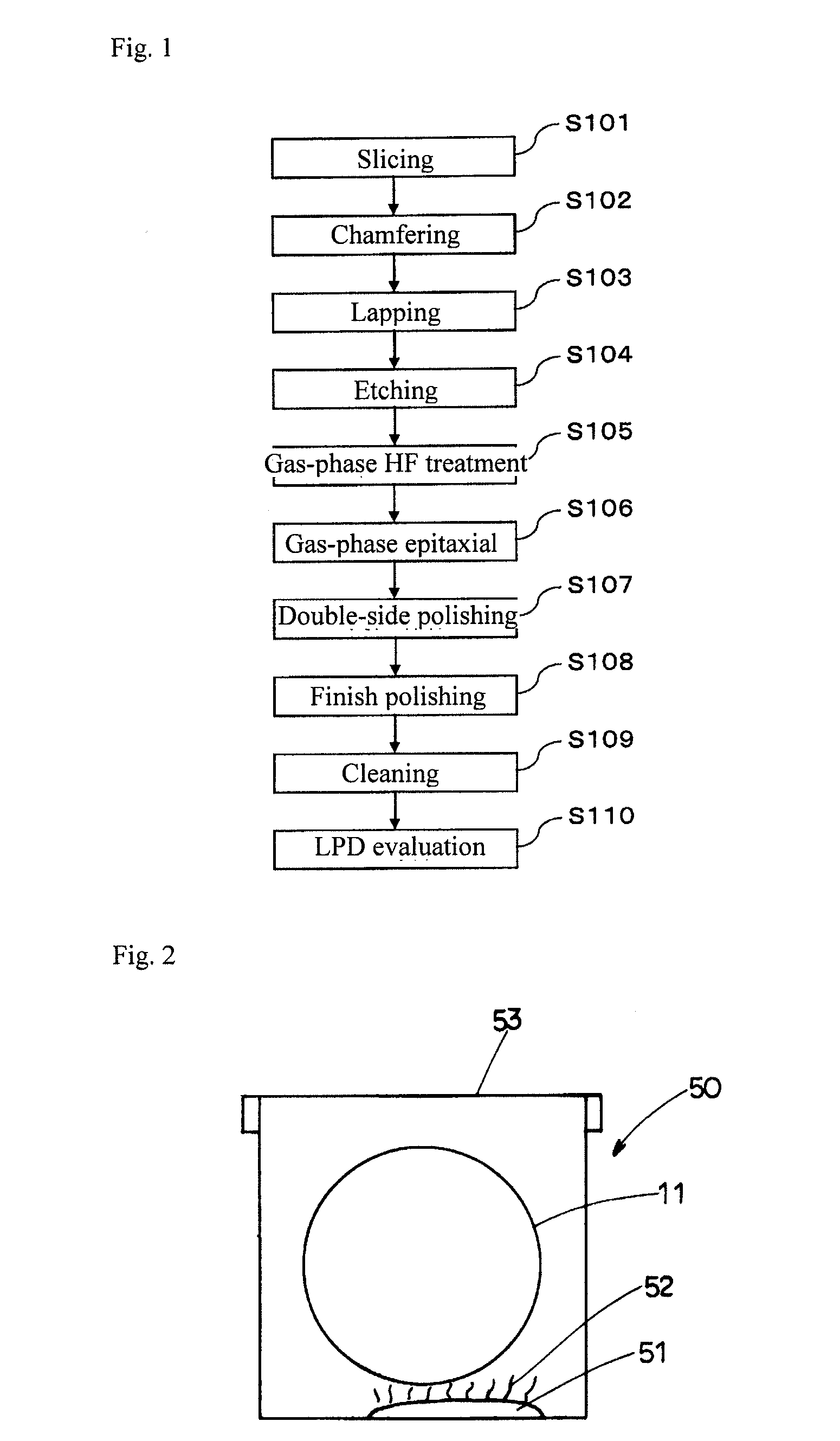
[0042]The silicon wafer is produced by sequentially performing processes below. Specifically, monocrystalline silicon is pulled in the CZ process from a silicon melt in a crucible doped with a predetermined amount of boron. The monocrystalline silicon is subsequently cut into blocks, ground on an external periphery, and then sliced into a plurality of wafers by a wire saw. Thereafter, each wafer is sequentially chamfered, lapped, etched, treated with gas-phase HF, epitaxially grown, double-side polished, finish polished, cleaned, and LPD evaluated....

second embodiment

[0056]A method of manufacturing an epitaxial silicon wafer according to the second embodiment of the present invention is explained with reference to FIG. 7. As shown in FIG. 7, the hydrogen fluoride gas 52 is sprayed from a spray nozzle 54 to the front surface of the silicon wafer 11 in the gas-phase HF treatment (S105) in the method of manufacturing the epitaxial silicon wafer according to the second embodiment. Specifically, one silicon wafer 11 is placed on a single-wafer type rotation table 56, and then the rotation table 56 is rotated at a rate of 300 to 500 rpm. One spray nozzle 54 is horizontally reciprocated above the rotation table 56 in a diameter direction of the rotation table 56 at 1 to 2 cm / second for a reciprocation distance of 120 cm. At the time, the hydrogen fluoride gas 52 is supplied from the spray nozzle 54 at a rate of 1 to 2 liter / minute for 4 to 5 minutes. A diameter extension cover 55 having a circular shape from a plan view is fixed to an end portion of th...


PUM

PropertyMeasurementUnit
thicknessaaaaaaaaaa
boiling pointaaaaaaaaaa
temperatureaaaaaaaaaa

Abstract

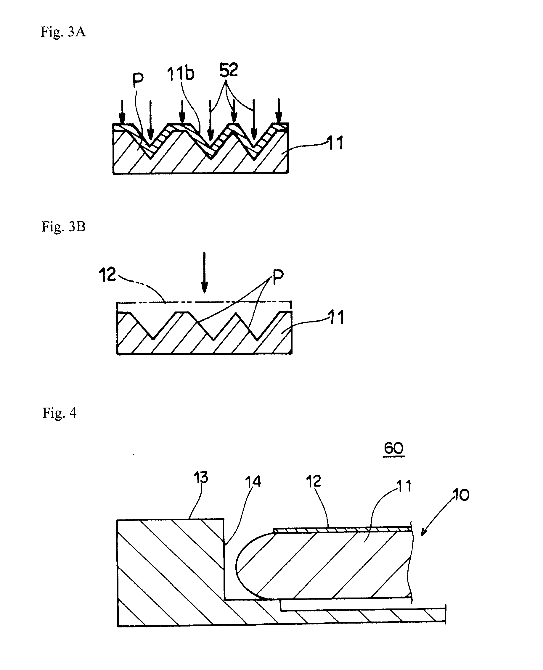
A silicon oxide film on a wafer front surface, including on internal surfaces of pits, is removed by hydrogen fluoride gas. The pits are thus completely filled with a film growth component at a time of epitaxial film growth. Thereby, productivity is not reduced; wafer flatness is enhanced; and micro-roughness of the wafer front surface is improved.

Description

BACKGROUND OF THE INVENTION[0001]1. Field of the Invention[0002]The present invention relates to a method of manufacturing an epitaxial silicon wafer, specifically a method of manufacturing an epitaxial silicon water capable of improving wafer flatness properties and wafer surface properties.[0003]2. Description of Related Art[0004]In a general manufacturing process of epitaxial silicon wafers, a front surface of a silicon wafer is mirror-polished, and then an epitaxial film is epitaxially grown (film growth) on the wafer front surface. In the method, however, unevenness in thickness of the epitaxial film occurs at the time of epitaxial growth, due to fluctuation of growth gas flow at the time of epitaxial growth. In addition, since source gas moves to a rear surface at the time of epitaxial growth, deposition occurs on the rear surface of the silicon wafer, thus causing a change in surface roughness (increase in a haze value). It is thus considered recently to polish the wafer fron...

Claims


Application Information

Patent Timeline
Patent Type & Authority Applications(United States)
IPC IPC(8): C30B23/02
CPCC30B29/06C30B33/12H01L21/02008H01L21/02661H01L21/02381H01L21/02532H01L21/02049
Inventor OKUUCHI, SHIGERU
Owner SUMCO CORP
Learn More