Semiconductor device having integrated mosfet and schottky diode and manufacturing method thereof

a technology of mosfet and diodes, which is applied in the direction of semiconductor devices, diodes, electrical apparatus, etc., can solve the problems of unavoidable parasitic inductance generation and higher production cost, and achieves higher efficiency, higher voltage tolerance, and high density

Inactive Publication Date: 2010-11-18
ANPEC ELECTRONICS CORPORATION
View PDF7 Cites 24 Cited by
  • Summary
  • Abstract
  • Description
  • Claims
  • Application Information

AI Technical Summary

Benefits of technology

[0007]The present invention therefore provides a TMBS and manufacturing method thereof ...

Problems solved by technology

But it suffers higher production cost and unavoidable parasitic inductances...

Method used


Image

  • Semiconductor device having integrated mosfet and schottky diode and manufacturing method thereof
  • Semiconductor device having integrated mosfet and schottky diode and manufacturing method thereof
  • Semiconductor device having integrated mosfet and schottky diode and manufacturing method thereof

Examples


Embodiment Construction

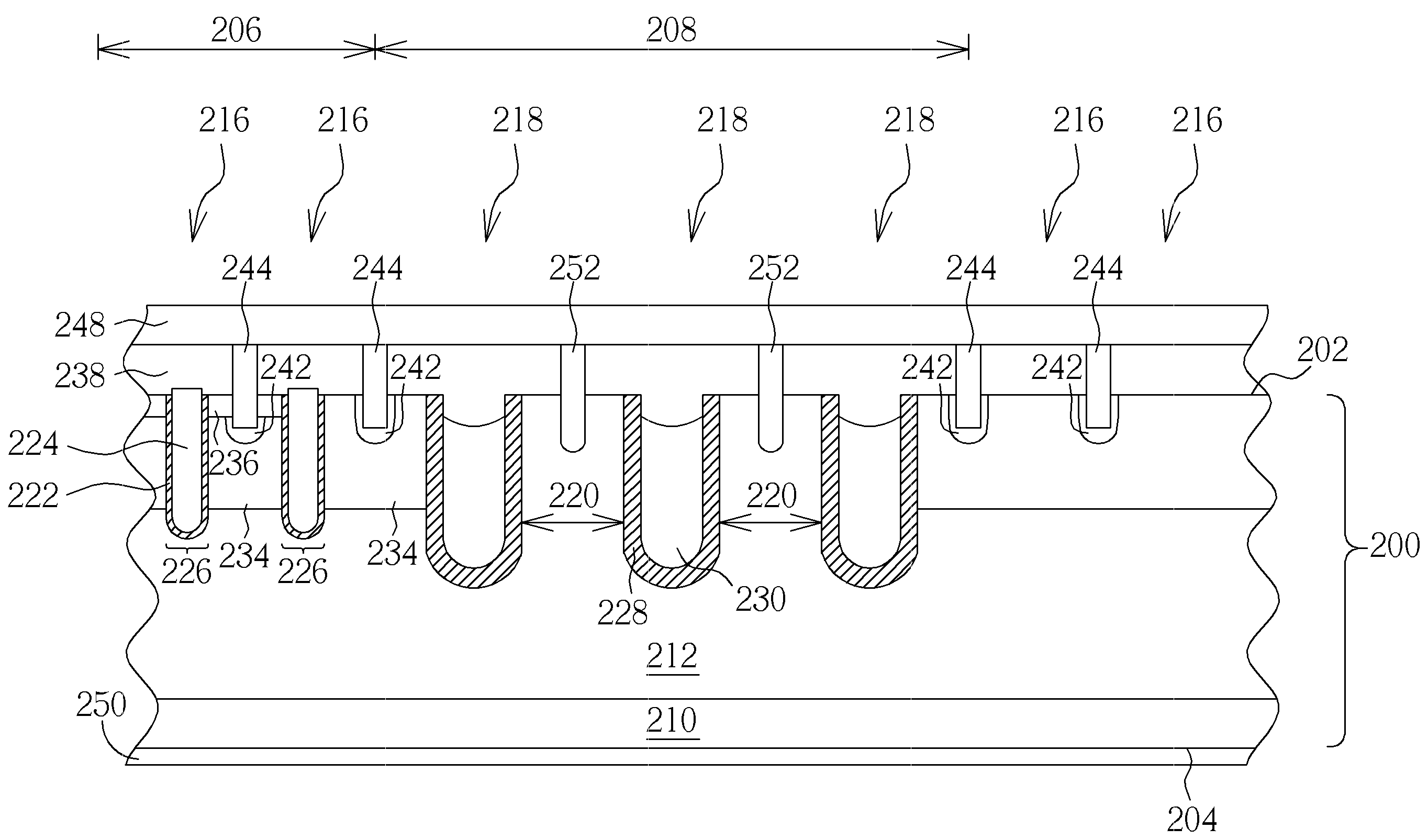
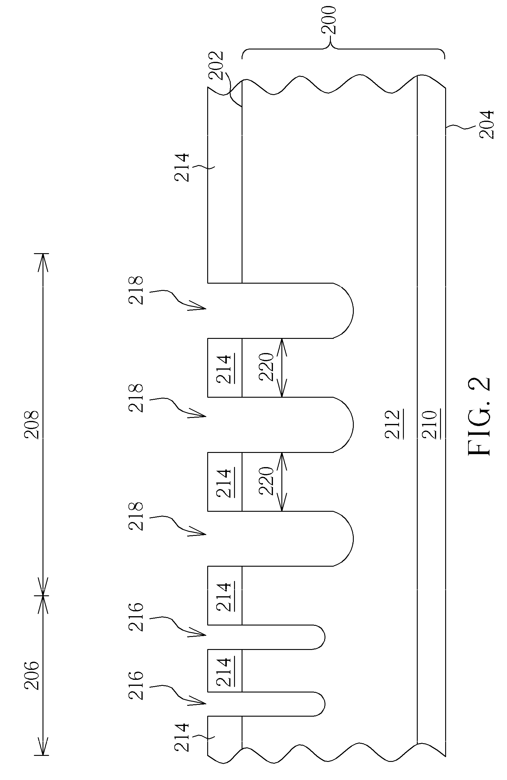
[0035]Please refer to FIGS. 2-10, which are schematic drawings illustrating a method of manufacturing a semiconductor device having integrated MOSFET and Schottky diode provided by a first preferred embodiment of the present invention. As shown in FIG. 2, a semiconductor substrate 200 is provided, the semiconductor substrate 200 includes a first surface 202 and a second surface 204 opposite to the first surface 202. The first surface 202 further includes a MOSFET region 206 and a Schottky diode region 208 defined thereon. The semiconductor substrate 200 comprises a silicon substrate 210 and an epitaxial silicon layer 212 formed over the silicon substrate 210. Both of the silicon substrate 210 and the epitaxial silicon layer 212 comprises a first dopant type. In the first preferred embodiment, the first dopant type is N-type. The silicon substrate 210 is heavily doped. In other words, a doped concentration of the silicon substrate 210 is higher than a doped concentration of the epita...


PUM


Abstract

A semiconductor device having integrated MOSFET and Schottky diode includes a substrate having a MOSFET region and a Schottky diode region defined thereon; a plurality of first trenches formed in the MOSFET region; and a plurality of second trenches formed in the Schottky diode region. The first trenches respectively including a first insulating layer formed over the sidewalls and bottom of the first trench and a first conductive layer filling the first trench serve as a trenched gate of the trench MOSFET. The second trenches respectively include a second insulating layer formed over the sidewalls and bottom of the second trench and a second conductive layer filling the second trench. A depth and a width of the second trenches are larger than that of the first trenches; and a thickness of the second insulating layer is larger than that of the first insulating layer.

Description

BACKGROUND OF THE INVENTION[0001]1. Field of the Invention[0002]This present invention is related to a semiconductor device having integrated metal-oxide-semiconductor field-effect transistor (MOSFET) and Schottky diode and manufacturing method thereof, and more particularly, to a semiconductor device having integrated trench MOS barrier Schottky (TMBS) and manufacturing method thereof.[0003]2. Description of the Prior Art[0004]A Schottky diode is constructed by a metal-to-semiconductor interface where this interface is known to have rectifying characteristics as a PN-junction diode. Moreover, Schottky diode provides rectification as a result of unipolar current transport across the metal-semiconductor contact. Consequently, the Schottky diode has advantage of lower threshold voltage and faster response speed when switching between forward and reverse bias voltage over the PN-junction diode. Thus Schottky diode is widely used in power converter for reducing power consumption and imp...

Claims


Application Information

Patent Timeline
IPC IPC(8): H01L27/06H01L21/8234H01L21/336
CPCH01L29/8725H01L27/0629
Inventor LIN, WEI-CHIEHLIN, LI-CHENGHSU, HSIN-YUCHEN, HO-TAIYEH, JEN-HAOYANG, GUO-LIANGCHEN, CHIA-HUIHUNG, SHIH-CHIEH
Owner ANPEC ELECTRONICS CORPORATION
Why Eureka
Try Eureka