Substrate having embedded single patterned metal layer, and package applied with the same, and methods of manufacturing of the substrate and package

Inactive Publication Date: 2010-11-18
ADVANCED SEMICON ENG INC
61 Cites 28 Cited by

AI-Extracted Technical Summary

Problems solved by technology

Thus, it is very difficult to achieve a high efficiency wiring on a BGA substrate or a lead frame substrate.
Besides, in addition to the request of the flip chip technology, the request of systematic integration of the downstream products is also getting more and more urgent.
However, plating procedure for filling the through hole requires more complicated technique and lon...

Method used

[0036]With a suitable carrier 20, this can be done on both sides to allow double sided processing for increased efficiency. Take the substrate formed on the upper side of the carrier 20 (FIG. 3G) for example. At least parts of the bottom surface of the patterned metal layer 301 are exposed by the pattern of the first patterned dielectric layer 303 so as to form several first contact pads 3015 for downward electrical connection externally. In particular applications, the first contact pads 3015 are ball pads, for being filled with a conductive material or attached by the solder balls (not shown) downwardly. The second patterned dielectric layer 305 at least exposes parts of the top surface of the patterned metal layer 301 to function as several second contact pads 3013 for upward electrical connection externally. In typical applications, the second contact pads 2021 are the bonding pads for conductive connection between the substrate and a die/chip of the package. Also, in one embodiment, each of the first patterned dielectric layers 303, 304 and the second patterned dielectric layers 305, 306 may include at least a slot opening so as to expose the first contact pads 3015 and the second contact pads 3013.
[0038]Moreover, the substrate of FIG. 3H may be further optionally subjected to a surface treatment to form the surface finish layers on the exposed surfaces of the patterned metal layer 301, thereby enhancing the electrical connection of the substrate. As shown in FIG. 3I, a first surface finish layer 308a (i.e. positioned between the holes of the second patterned dielectric layer 305) is formed on the surfaces of the second contact pads 3013, and a second surface finish layer 308b (i.e. positioned between the apertures of the first patterned dielectric layer 303) is formed on the surfaces of the first contact pads 3015. Also, materials chosen for making the first surface finish layer 308a and the second surface finish layer 3...

Benefits of technology

[0012]The present invention provides structures of the substrate having a single patterned metal layer, and the package with this substrate, and methods of manufacturing the same. The substrate of the disclosure merely includes a patterned metal layer (as conductive traces) and two dielectric layers, which reduces the thickness of the substrate. This extra thin substrate is par...

Abstract

A substrate having single patterned metal layer applied in a package is provided. The substrate includes a first patterned dielectric layer, a patterned metal layer and a second patterned dielectric layer, wherein the patterned metal layer is embedded in the first patterned dielectric layer. Also, the top surfaces of the patterned metal layer and the first patterned dielectric layer lie in the same plane. At least part of the patterned metal layer are exposed from the holes formed on the lower surface of the first patterned dielectric layer, so as to form plural first contact pads for electrical connection downwardly. The second patterned dielectric layer, formed above the patterned metal layer and the first patterned dielectric layer, at least exposes part of the patterned metal layer to form plural second contact pads at the top surface of the patterned metal layer for electrical connection upwardly.

Application Domain

Technology Topic

Image

  • Substrate having embedded single patterned metal layer, and package applied with the same, and methods of manufacturing of the substrate and package
  • Substrate having embedded single patterned metal layer, and package applied with the same, and methods of manufacturing of the substrate and package
  • Substrate having embedded single patterned metal layer, and package applied with the same, and methods of manufacturing of the substrate and package

Examples

  • Experimental program(2)

Example

FIRST EMBODIMENT
[0027]FIG. 3A˜FIG. 3I schematically show a progressive flow of manufacturing a substrate having single patterned metal layer according to the first embodiment of the present invention. First, a structure of an embedded patterned metal layer is formed. In the first embodiment, a carrier is used for an implement to complete the fabrication of the patterned metal layer.
[0028]As shown in FIG. 3A, a carrier 20 with the metal foils 201 and 202 on its opposites surfaces is provided. In one embodiment, a copper foil having a thickness of about 12 μm can be used as the metal foil.
[0029]As shown in FIG. 3B, the patterned metal layers 301 and 302 are then formed on the metal foils 201 and 202, respectively. Formation of the patterned metal layers 301 and 302 could be done by the following steps. Two metal layers are formed on the metal foils 201 and 202, respectively. Then, a dry film is formed on the metal layer followed by exposing and developing to form a patterned dry film on each sides of the carrier 20. The metal layers are etched according to the patterned dry films to form the patterned metal layers 301 and 302. Finally, the patterned dry films are removed.
[0030]Afterwards, the first patterned dielectric layers 303 and 304 are formed on the bottom surfaces of the patterned metal layers 301 and 302, respectively. Also, there are several apertures 303a, 303b formed at the bottom surface of the first patterned dielectric layer 303 to expose parts of the bottom surface of the patterned metal layer 301, as shown in FIG. 3C. Similarly, there are several apertures 304a, 304b formed at the bottom surface of the first patterned dielectric layer 304 to expose parts of the bottom surface of the patterned metal layer 302.
[0031]Then, the transitional structures 41 and 42 formed so far are removed from the carrier 20, as shown in FIG. 3D. The transitional structure 41 comprises the metal foil 201, the patterned metal layer 301 and the first patterned dielectric layer 303. Similarly, the transitional structure 42 on the other side of the carrier 20 comprises the metal foil 202, the patterned metal layer 302 and the first patterned dielectric layer 304.
[0032]Subsequently, the transitional structures 41 and 42 are removed from the carrier 20 and re-placed inversely on the carrier 20, so that the bottom surfaces of the first patterned dielectric layers 303 and 304 are respectively disposed on the carrier 20, as shown in FIG. 3E.
[0033]Then, the metal foils 201 and 202 are removed, as shown in FIG. 3F. It is indicated that the top surface of the patterned metal layer 301 is coplanar with the top surface of the first patterned dielectric layer 303. Similarly, the pattern on the other side of the carrier 20 has indicated that the top surface of the patterned metal layer 302 is coplanar with the top surface of the first patterned dielectric layer 304. Accordingly, the patterned metal layers 301 and 302 are embedded in the first patterned dielectric layers 303 and 304, respectively.
[0034]Afterwards, as shown in FIG. 3G, a second patterned dielectric layer 305 is formed on the top surfaces of the patterned metal layer 301 and the first patterned dielectric layer 303. Similarly, the other second patterned dielectric layer 306 is formed on the top surfaces of the patterned metal layer 302 and the first patterned dielectric layer 304. Also, the second patterned dielectric layers 305 and 306 have several through holes 305a, 305b, 306a and 306b to expose parts of the top surfaces of the patterned metal layers 301 and 302, respectively.
[0035]Then, the structures formed so far are removed from the carrier 20, as shown in FIG. 3H.
[0036]With a suitable carrier 20, this can be done on both sides to allow double sided processing for increased efficiency. Take the substrate formed on the upper side of the carrier 20 (FIG. 3G) for example. At least parts of the bottom surface of the patterned metal layer 301 are exposed by the pattern of the first patterned dielectric layer 303 so as to form several first contact pads 3015 for downward electrical connection externally. In particular applications, the first contact pads 3015 are ball pads, for being filled with a conductive material or attached by the solder balls (not shown) downwardly. The second patterned dielectric layer 305 at least exposes parts of the top surface of the patterned metal layer 301 to function as several second contact pads 3013 for upward electrical connection externally. In typical applications, the second contact pads 2021 are the bonding pads for conductive connection between the substrate and a die/chip of the package. Also, in one embodiment, each of the first patterned dielectric layers 303, 304 and the second patterned dielectric layers 305, 306 may include at least a slot opening so as to expose the first contact pads 3015 and the second contact pads 3013.
[0037]In one embodiment, materials of the first patterned dielectric layers 303, 304 and the second patterned dielectric layers 305, 306 may be optionally selected from solder mask (SM), liquid crystal polymer (LCP), prepreg (PP), molding compounds, or other dielectric materials. Also, materials of the first patterned dielectric layers 303, 304 and the second patterned dielectric layers 305, 306 may be the same or different. The materials and selections of the first and second patterned dielectric layers 303-306 are not intended to be limited to these illustrative compounds.
[0038]Moreover, the substrate of FIG. 3H may be further optionally subjected to a surface treatment to form the surface finish layers on the exposed surfaces of the patterned metal layer 301, thereby enhancing the electrical connection of the substrate. As shown in FIG. 3I, a first surface finish layer 308a (i.e. positioned between the holes of the second patterned dielectric layer 305) is formed on the surfaces of the second contact pads 3013, and a second surface finish layer 308b (i.e. positioned between the apertures of the first patterned dielectric layer 303) is formed on the surfaces of the first contact pads 3015. Also, materials chosen for making the first surface finish layer 308a and the second surface finish layer 308b could be identical or different. In the present embodiment, materials of the first and second surface finish layers 308a and 308b are independently selected from the group consisting of Ni/Au, NiPdAu, Ni/Ag, Au, Tin, Tin-lead alloy, silver, OSP and combination thereof. Alternatively, the final surface treatments for the first and second contact pads can be done by selective plating of electroless nickel/electroless palladium/immersion gold (ENEPIG) and OSP depending on the requirements of applications. Moreover, in one embodiment, the first surface finish layer 308a formed on the second contact pads 3013 is spaced apart from the sidewalls of the second patterned dielectric layer 305, as illustrated by the distances d1 and d2 of FIG. 3I. These distances d1 and d2 could be identical or different, depending on the requirements of applications.
[0039]FIG. 4 depicts a package with the substrate of FIG. 3I manufactured according to the first embodiment of the present invention. Package 61 includes the substrate as presented in FIG. 3I, a die 602 disposed on the second patterned dielectric layer 305, the bonding wires 603a, 603b, and a molding compound 607. Lower surface of the die 602 is attached to the second patterned dielectric layer 305 with an adhesive material 601 (such as epoxy). The active surface of the die 602 is electrically connected to the first surface finish layer 308a on the second contact pads 3013 through the bonding wires 603a, 603b. The molding compound 607 is applied onto the first patterned dielectric layer 303 to cover the first patterned dielectric layer 303, the patterned metal layer 301, the second patterned dielectric layer 305, the die 602, and the bonding wires 603a, 603b. The material selected for molding compound 607 should be electrically insulating, such as epoxy.
[0040]According to the above descriptions, the patterned metal layer 301 of the substrate, as shown in FIG. 3I and FIG. 4, is embedded in the first patterned dielectric layer 303, and the top surface of the patterned metal layer 301 is aligned with the top surface of the first patterned dielectric layer 303. The second patterned dielectric layer 305 is then formed on the patterned metal layer 301. Compared to the prior art, the substrate structure of the disclosure merely includes two patterned dielectric layers (303/305) and a single patterned metal layer (as conductive traces). The substrate fabricated according to the first embodiment is very thin, having a thickness ranged from about 40 μm to about 130 μm. The package size applied with the substrate of the first embodiment can be effectively kept to a minimum with this combination. This extra thin substrate is particularly suitable for the application of small-sized product. Also, the method disclosed in the first embodiment not only makes the substrate with smaller trace pitch, but also simplifies the substrate manufacturing process.
[0041]Although FIG. 3A˜FIG. 3H demonstrate the method of manufacturing the substrates progressing at both sides of the carrier for increasing the production rate, it is not intended to limit the invention to these illustrative sense. The method of manufacturing the substrate can be progressed at single sides of the carrier 20 as required by practical applications.

Example

SECOND EMBODIMENT
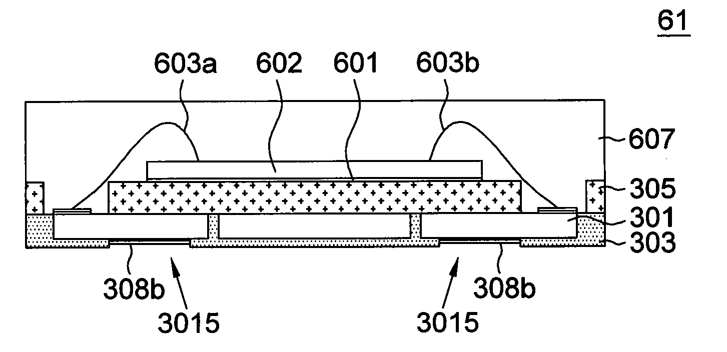
[0042]Besides substrate 51 of the first embodiment (FIG. 3I), the substrate structure can be varied by slightly modifying the methods described above without departing from the spirit of the invention. FIG. 5A is a cross-sectional view of an alternative substrate manufactured according to the second embodiment of the present invention. The features of the second embodiment identical to the features of the first embodiment are designated with the same reference numbers.
[0043]The method of fabricating the substrate 52 of FIG. 5A could be referred to the process as demonstrated in FIG. 3A˜FIG. 3H. Substrate 52 of FIG. 5A is similar to substrate 51 of FIG. 3I except the die being disposed on the portion of the patterned metal layer 301. In the second embodiment, the patterned metal layer 301 includes a die supporting pad 2071, several first contact pads 3015 (ex: bonding pads) and the second contact pads 3013 (ex: ball pads). Furthermore, the second patterned dielectric layer 305 of the second embodiment has a die-receiving area 522 corresponding to the position of the die supporting pad 3017. As shown in FIG. 5A, the die-receiving area 522 completely exposes the die supporting pad 3017.
[0044]FIG. 5B depicts a package with the substrate of FIG. 5A manufactured according to the second embodiment of the present invention. Package 62 includes the substrate as presented in FIG. 5A, a die 602, the bonding wires 603a, 603b, and a molding compound 607. Lower surface of the die 602 is attached to the die supporting pad 3017 of the patterned metal layer 301 within a die-receiving area 522 with an adhesive material 601 (such as epoxy). The active surface of the die 602 is electrically connected to the first surface finish layer 308a on the second contact pads 3013 through the bonding wires 603a, 603b. The molding compound 607 is applied onto the first patterned dielectric layer 303 to cover the first patterned dielectric layer 303, the patterned metal layer 301, the second patterned dielectric layer 305, the die 602, and the bonding wires 603a, 603b. As shown in FIG. 5B, the thickness h2 of the die 602 is smaller than the thickness h1 of the second patterned dielectric layer 305, thereby reducing the overall thickness of the package.
[0045]Similarly, the patterned metal layer 301 of the substrate, as shown in FIG. 5A and FIG. 5B, is embedded in the first patterned dielectric layer 303, and the top surface of the patterned metal layer 301 is aligned with the top surface of the first patterned dielectric layer 303. Compared to the prior art, the substrate structure of the disclosure merely includes two patterned dielectric layers (303/305) and a single patterned metal layer (as conductive traces). The substrate fabricated according to the first embodiment is very thin, and the package size applied with the substrate of the embodiment can be effectively kept to a minimum with this combination. This extra thin substrate is particularly suitable for the application of small-sized product.
[0046]Although two types of substrates 61, 62, and packages 71 and 72 have been illustrated with reference to specific embodiments, it is noted that the final structure of the substrate can be variable in accordance with requirements of the practical application. For example, the die could be wire bonded or flipped bonded to the substrate. Also, materials and patterns of the metal layer and dielectric layer would be varied from the illustration, depending to the specific requirements of the device. Those skilled in the art will recognize that modifications and variations can be made without departing from the spirit of the invention.
[0047]The foregoing description and illustrations contained herein demonstrate many of the advantages associated with the present embodiments over the prior art. By providing substrate having two patterned dielectric layers and a patterned metal layer, the thickness of the substrate is reduced to about 40 μm-130 μm giving rise to a lower profile package. This extra thin substrate is particularly suitable for the application of small-sized product. Also, the methods for manufacturing the substrates and packages disclosed in the foregoing embodiments are simple and suitable for mass production which has advantages of low cost and high yield of production. Compared to the prior art, the substrate structure of the disclosure satisfies the desired requirements of the electronic product with thin profile and low cost. Thus, the electronic product applied with the substrate of the present embodiment, especially for the small-sized and low-priced product, is very competitive in the commercial market.
[0048]While the invention has been described by way of example and in terms of the preferred embodiment, it is to be understood that the invention is not limited thereto. On the contrary, it is intended to cover various modifications and similar arrangements and procedures, and the scope of the appended claims therefore should be accorded the broadest interpretation so as to encompass all such modifications and similar arrangements and procedures.

PUM

PropertyMeasurementUnit
Thickness4.0E-5m
Thickness1.3E-4m
Dielectric polarization enthalpy
tensileMPa
Particle sizePa
strength10

Description & Claims & Application Information

We can also present the details of the Description, Claims and Application information to help users get a comprehensive understanding of the technical details of the patent, such as background art, summary of invention, brief description of drawings, description of embodiments, and other original content. On the other hand, users can also determine the specific scope of protection of the technology through the list of claims; as well as understand the changes in the life cycle of the technology with the presentation of the patent timeline. Login to view more.

Similar technology patents

Airfoil for a helicoptor rotor blade

ActiveUS20070187549A1Reduce thicknessReduce camberWing shapesDrag reductionEngineeringHigh lift
Owner:SIKORSKY AIRCRAFT CORP

Classification and recommendation of technical efficacy words

  • High production yield
  • Reduce thickness

Preparation and application of novel dual-core organic skeleton material MIL-100(Fe-Mn)

InactiveCN105237586AExcellent surface adsorption and chemical reactivityHigh production yieldOrganic chemistryOrganic-compounds/hydrides/coordination-complexes catalystsChemistrySmoke
Owner:DALIAN UNIV OF TECH

Preparation Method Of Solid Titanium Catalyst For Olefin Polymerization

InactiveUS20070298964A1Production yield be raiseHigh production yieldMechanical apparatusLighting and heating apparatusOlefin polymerizationMagnesium
Owner:SAMSUNG TOTAL PETROCHEMICALS CO LTD
Why Eureka
Try Eureka