Electronic component, manufacturing method for electronic component, and electronic device

a manufacturing method and electronic component technology, applied in the direction of printed circuit non-printed electric components, semiconductor/solid-state device details, electrical apparatus casings/cabinets/drawers, etc., can solve the problems of reduced solder joint strength, prone to cracking, brittle intermetallic compound layer, etc., and achieve high solderability

Active Publication Date: 2010-11-18
SEIKO INSTR INC
View PDF27 Cites 41 Cited by
  • Summary
  • Abstract
  • Description
  • Claims
  • Application Information

AI Technical Summary

Benefits of technology

[0032]According to the present invention, an intermetallic compound layer is absent at the interface between the electrode metal layer and the jo

Problems solved by technology

The intermetallic compound layer is brittle compared with a base material, and hence has a problem of being prone to crack when applied with an external force.
In addition, the intermetallic compound layer grows when heated to high temperature, and hence if the Ni layer or the Cu layer completely reacts with Sn in the solder, solder joint strength is reduced, which poses a problem that the Ni layer or the Cu layer needs to have a certain degree of thickness.
If the technology of JP

Method used


Image

  • Electronic component, manufacturing method for electronic component, and electronic device
  • Electronic component, manufacturing method for electronic component, and electronic device
  • Electronic component, manufacturing method for electronic component, and electronic device

Examples


Embodiment Construction

[0050](1) Summary of Embodiment

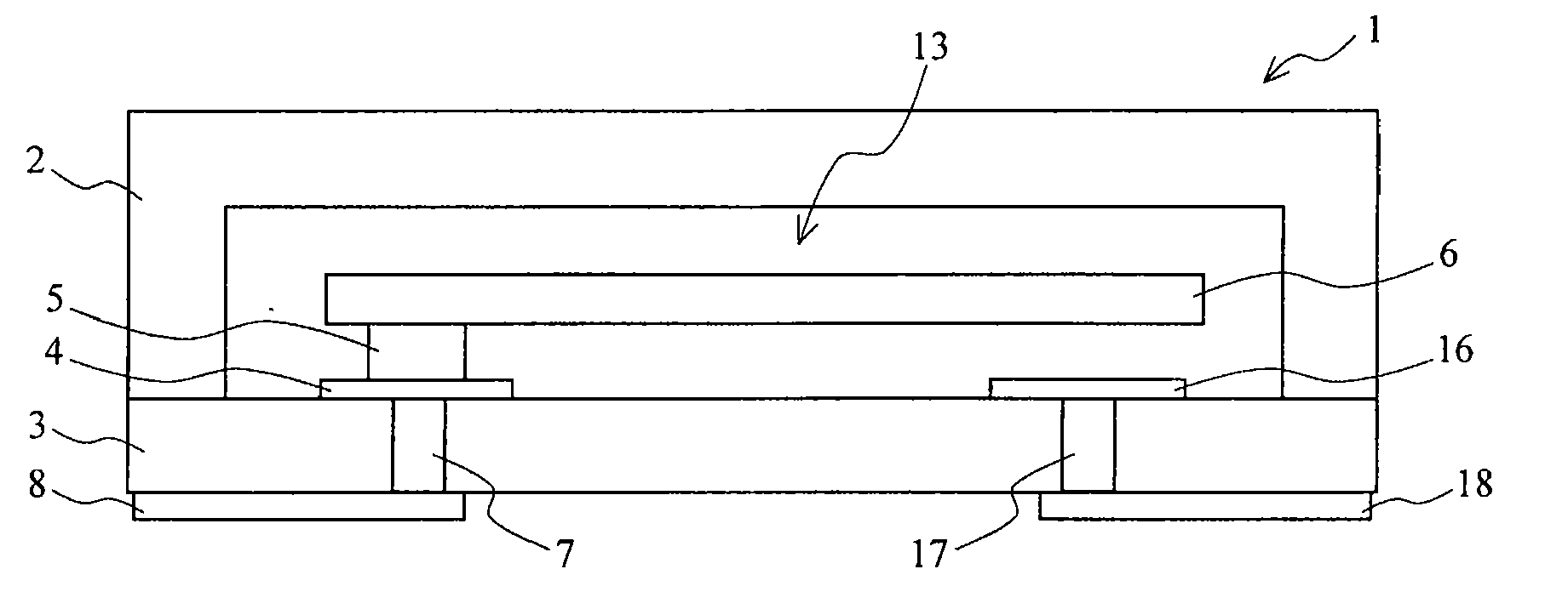
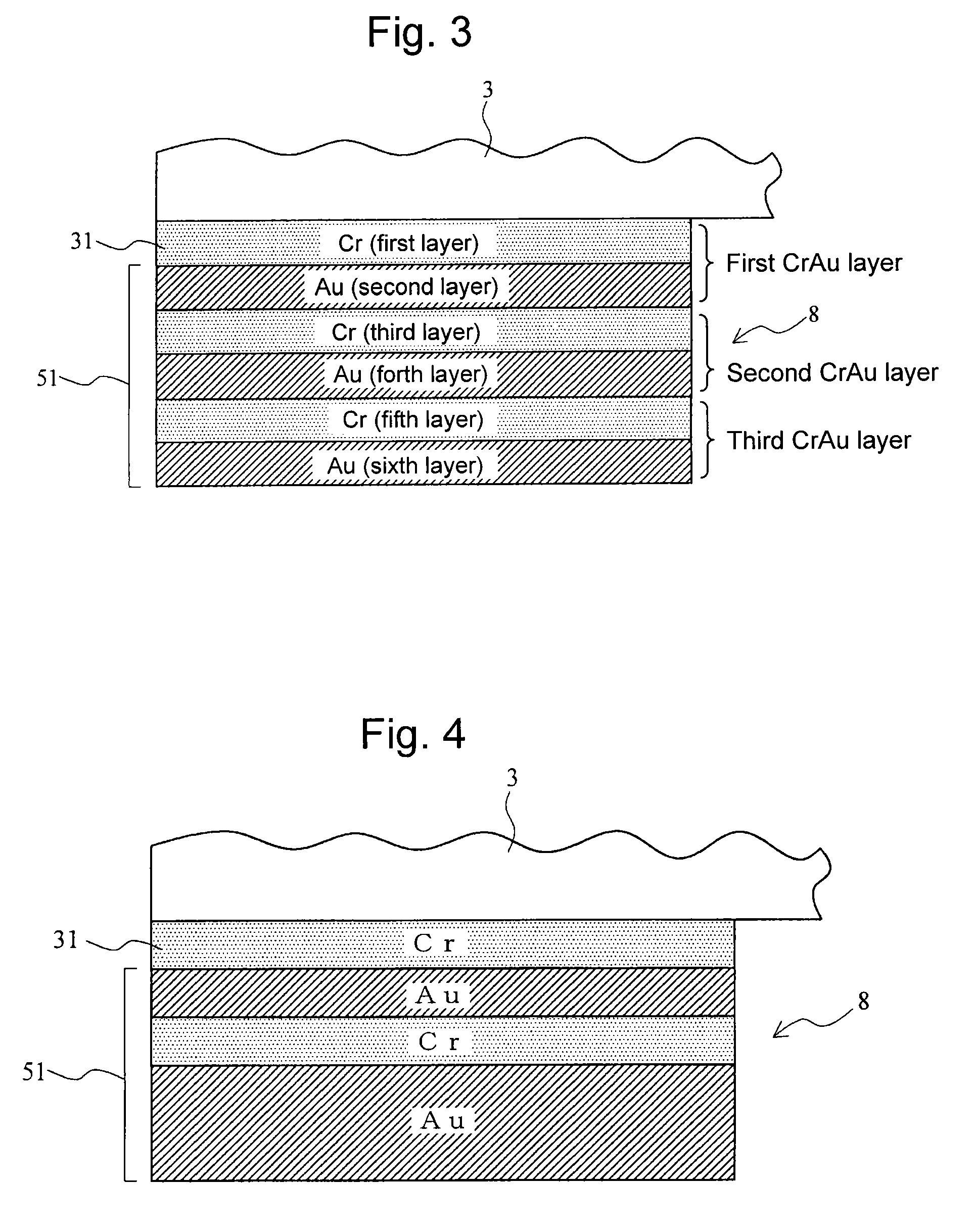
[0051]An electronic device has electronic elements installed therein. Outer electrodes are formed on a bottom surface of a glass package that houses the electronic element therein. The outer electrodes each include an electrode metal layer that is bonded to a glass-made base, and a surface layer that is formed on a surface of the electrode metal layer. The electrode metal layer is made of a metallic element, such as chromium (Cr), titanium (Ti), molybdenum (Mo), tungsten (W), or tantalum (Ta), which has good adhesive properties on glass and hardly forms a compound with solder (whose main component is tin (Sn)) under a temperature range for use. The surface layer is made of a metal, such as gold (Au), silver (Ag), or palladium (Pd), which resists oxidation under a temperature range for use, and easily dissolves into liquid solder in soldering.

[0052]It is revealed through an experiment described later that, when an outer electrode formed of such an elect...


PUM

PropertyMeasurementUnit
Thicknessaaaaaaaaaa
Thicknessaaaaaaaaaa
Nanoscale particle sizeaaaaaaaaaa

Abstract

To provide an improved solderability for mounting an electronic component onto a circuit board, a package of an electronic component (1) is formed by bonding together a base (3) made of glass and a lid (2). Outer electrodes (8) and (18) are formed on a bottom surface of the base (3), and the outer electrodes (8) and (18) are respectively connected to through electrodes (7) and (17). The outer electrodes (8) and (18) each have a laminated structure of three CrAu layers, that is, from a Cr layer (first layer) to an Au layer (sixth layer). When the outer electrodes (8) and (18) are soldered onto a circuit board, the Au layers as the second, fourth, and sixth layers are dissolved into solder, whereas the Cr layers as the third and fifth layers, which hardly form an intermetallic compound with solder, are separated to remain in solder.

Description

RELATED APPLICATIONS[0001]This application claims priority under 35 U.S.C. §119 to Japanese Patent Application Nos. 2009-116886, 2009-116887, and 2009-116888 all filed on May 13, 2009, the entire contents of which are hereby incorporated by reference.BACKGROUND OF THE INVENTION[0002]1. Field of the Invention[0003]The present invention relates to an electronic component, a manufacturing method for an electronic component, and an electronic device, and to, for example, an electronic component, a manufacturing method for an electronic component, and an electronic device having improved solderability for mounting an electronic component onto a circuit board.[0004]2. Description of the Related Art[0005]Some electronic elements, such as crystal resonators and semiconductors, are made available after being enclosed in packages. Each package has outer electrodes formed thereon, and the outer electrodes are soldered onto a circuit board so that an electronic element may be electrically and p...

Claims


Application Information

Patent Timeline
IPC IPC(8): H05K5/00H01L23/48H05K13/00
CPCH01L23/055Y10T29/49002Y10T29/49124H01L2924/19041H01L2924/0002H01L2924/00
Inventor TAKEUCHI, HITOSHISATO, KEIJIARATAKE, KIYOSHINUMATA, MASASHINAKAMURA, TAKAHIKOTERADA, DAISUKESUGIYAMA, TAKESHI
Owner SEIKO INSTR INC
Why Eureka
Try Eureka