Method for manufacturing acoustic wave device

a manufacturing method and technology of acoustic waves, applied in the direction of piezoelectric/electrostrictive transducers, transducer types, coatings, etc., can solve the problems of deterioration in line width processing accuracy, peeling of bonded surfaces, cracks in substrates, etc., to enhance tcf, excellent temperature coefficient of frequency, and increase rigidity of thermal spray films

Active Publication Date: 2010-11-25
MURATA MFG CO LTD
View PDF8 Cites 8 Cited by
  • Summary
  • Abstract
  • Description
  • Claims
  • Application Information

AI Technical Summary

Benefits of technology

[0014]Preferably, the method for manufacturing the acoustic wave device according to the present invention further comprises a step of filling pores in the film formed by thermal spraying with a filling material. According to this method, the rigidity of the thermal spray film is increased to enhance the TCF.
[0015]According to the method for manufacturing an acoustic wave device of the present invention, the IDT is formed on one principal surface of the piezoelectric substrate and a film is

Problems solved by technology

When a bonded substrate formed of a piezoelectric substrate and a substrate for temperature compensation bonded together is set in the wafer process or, for example, when an IDT for an acoustic wave device is formed on the bonded substrate, there occurs, in a heating step of the process, a stress due to a difference in linear thermal expansion coefficient between the piezoelectric

Method used


Image

  • Method for manufacturing acoustic wave device
  • Method for manufacturing acoustic wave device
  • Method for manufacturing acoustic wave device

Examples


example 1

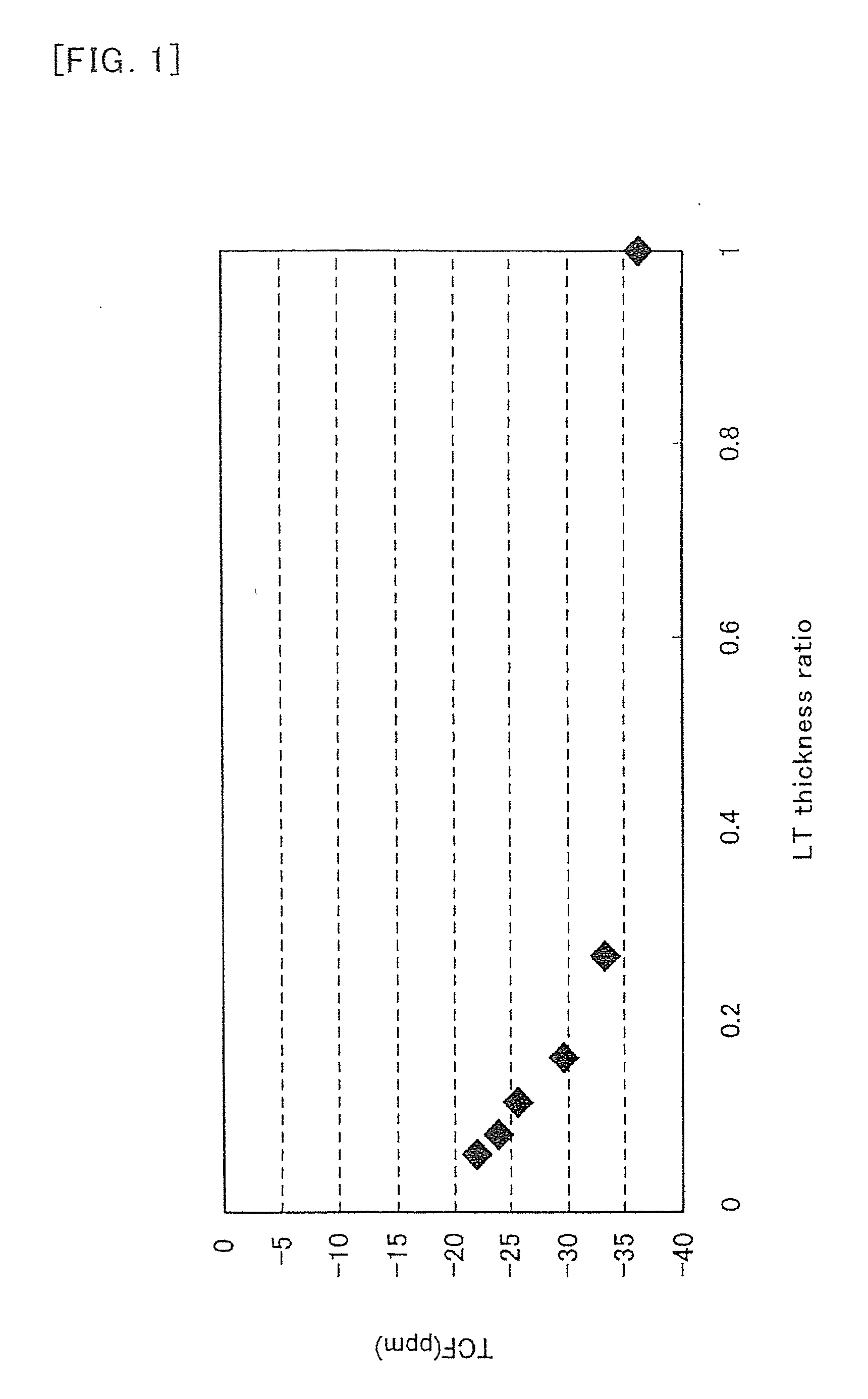
[0040]A substrate of lithium tantalate (LT substrate) was provided having a linear thermal expansion coefficient of 16×10−6 / K and a thickness of 0.02 mm, and mullite having a linear thermal expansion coefficient of 1×10⁻⁶ / K was thermal sprayed on one principal surface of the substrate at a thickness of 0.33 mm, thereby forming a 4-inch substrate. This 4-inch substrate was subjected to heating. Then, the 4-inch substrate was not cracked at heating temperatures of 180 and 200 degrees, however it was cracked at heating temperatures of 250 and 350 degrees.

[0041]Besides, instead of the LT substrate, a substrate of lithium niobate (LN substrate) having a linear thermal expansion coefficient of 15×10−6 / K and a thickness of 0.02 mm was used thereby to form a 4-inch substrate in the same way as mentioned above. This 4-inch substrate was subjected to heating. Then, the 4-inch substrate was not cracked at the heating temperatures of 180 and 200 degrees, however, it was cracked at the heating t...

example 2

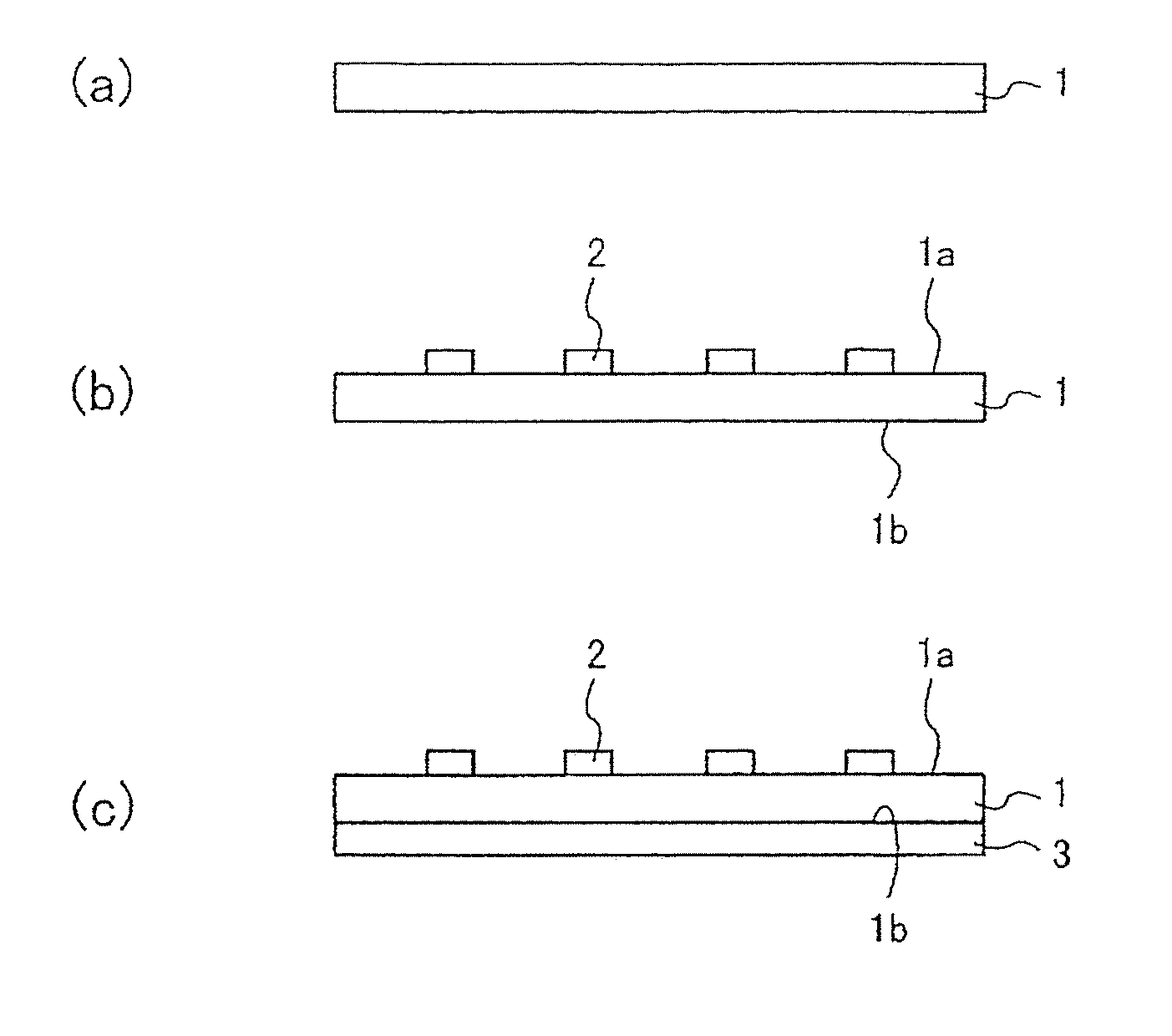
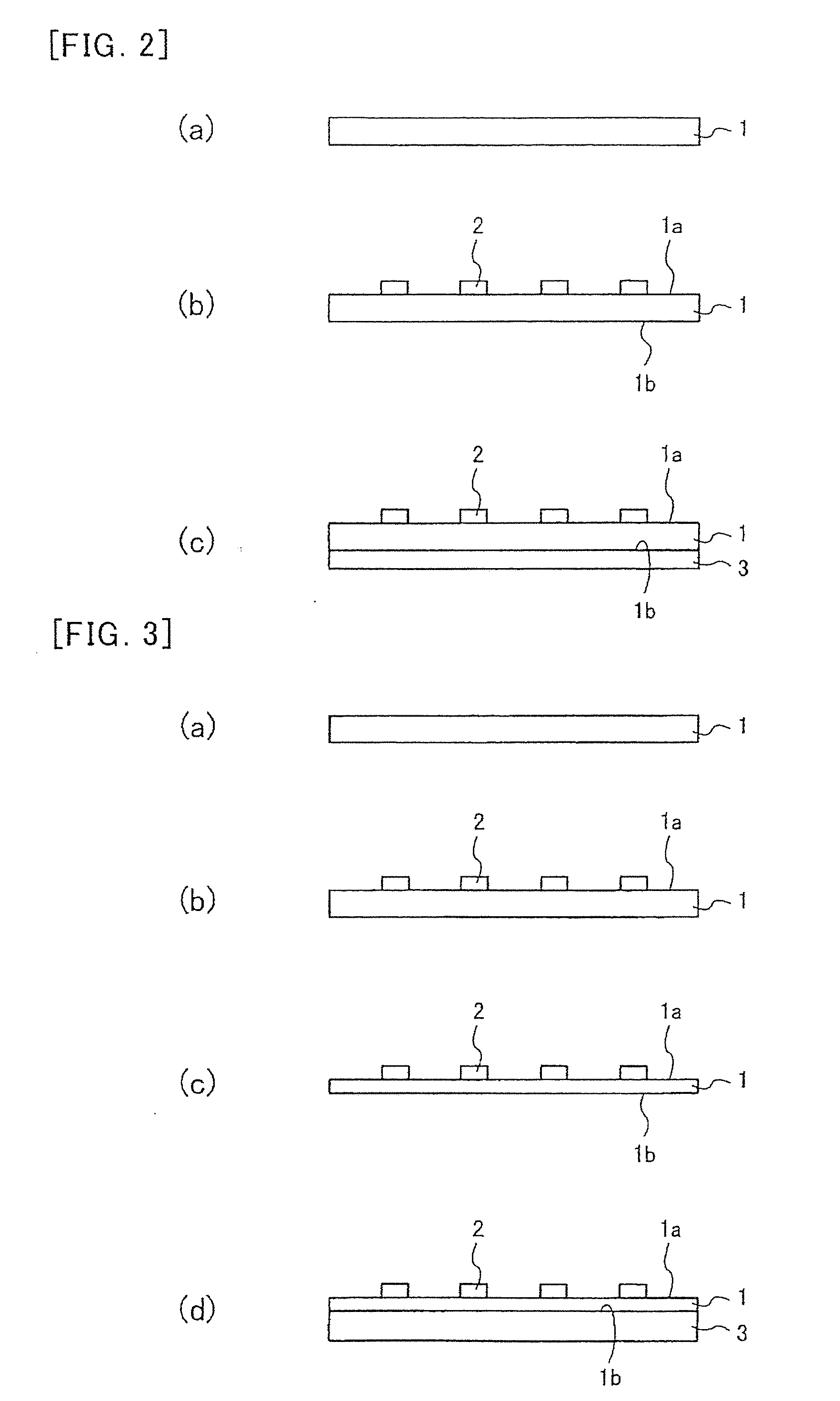
[0045]An IDT was formed on one principal surface of a substrate of lithium tantalate (LT substrate) having a linear thermal expansion coefficient of 16×10−6 / K, a diameter of 4 inches and a thickness of 0.25 mm. In this IDT forming, the resist used was a chemical amplification resist and the PEB (Post Exposure Bake) temperature was 110 degrees. Then, the opposite principal surface of the LT substrate was lapped to a thickness of 0.01 to 0.04 mm and roughened at Ra of 0.1 μm. Next, powders of silicon and alumina were thermal sprayed in this order on the roughened opposite principal surface so that a total thickness of the LT substrate and the thermal spray film was 0.25 mm. Here, the thermal spraying was performed with use of a DC plasma thermal spray device using Ar plasma gas and at power supply output of 40 kW.

[0046]The thus obtained wafer with IDT was examined as to the accuracy R of line width processing in the surface. This accuracy R was measured with an SEM (Scanning Electron ...


PUM

PropertyMeasurementUnit
Lengthaaaaaaaaaa
Lengthaaaaaaaaaa
Angleaaaaaaaaaa

Abstract

Provided is a method for manufacturing an acoustic wave device that has an excellent temperature coefficient of frequency (TCF) and high accuracy of IDT pattern forming and is capable of resisting high temperature processing of 200 degrees or more. The method for manufacturing an acoustic wave device according to the present invention includes forming an IDT (2) on a principal surface (1a) of a piezoelectric substrate (1), and forming a film by thermal spraying a material (3) having a smaller linear thermal expansion coefficient than the piezoelectric substrate onto an opposite principal surface (1b) of the piezoelectric substrate (1) where the IDT (2) is formed.

Description

TECHNICAL FIELD[0001]The present invention relates to a method for manufacturing an acoustic wave device such as a surface acoustic wave (SAW) device and a boundary acoustic wave device.BACKGROUND ART[0002]The acoustic wave device is a device having an inter-digital transducer (IDT) formed on a piezoelectric substrate such as lithium tantalate (LiTaO3:LT) substrate or lithium niobate (LiNbO3:LN) substrate. The LT and LN have high thermal expansion coefficients that are six times higher than the thermal expansion coefficient of silicon (the thermal expansion coefficients of LT and LN are about 16×10−6 / K and 15×10−6 / K, respectively, while the thermal expansion coefficient of silicon is about 2.6×10⁻⁶ / K). Then, if the LT or LN substrate is used in the acoustic wave device, there arises a significant problem of change in filtering performance due to temperature change. Therefore, temperature compensation is performed in various methods.[0003]For example, the patent document 1 discloses ...

Claims


Application Information

Patent Timeline
IPC IPC(8): H04R17/00
CPCH03H3/10H03H9/02559C23C4/10H03H3/02Y10T29/42C23C4/06H03H3/007C23C4/04H03H3/04Y10T29/49147Y10T29/49155
Inventor FUYUTSUME, TOSHIYUKINISHINO, TAROYAMAZAKI, HISASHITAMURA, NOBORUICHIKAWA, NAKABAARUGA, MASAKI
Owner MURATA MFG CO LTD
Why Eureka
Try Eureka