

Semiconductor light-emitting element and method for fabricating the same
a technology of semiconductors and light-emitting elements, which is applied in the direction of semiconductor devices, lasers, semiconductor lasers, etc., can solve the problems of unobtainable luminous efficiency and still left, and achieve excellent luminous efficiency, increase the effect of the present invention, and reduce thermal damage on the active layer
- Summary
- Abstract
- Description
- Claims
- Application Information
AI Technical Summary
Benefits of technology
Problems solved by technology
Method used
Image

Examples
second embodiment
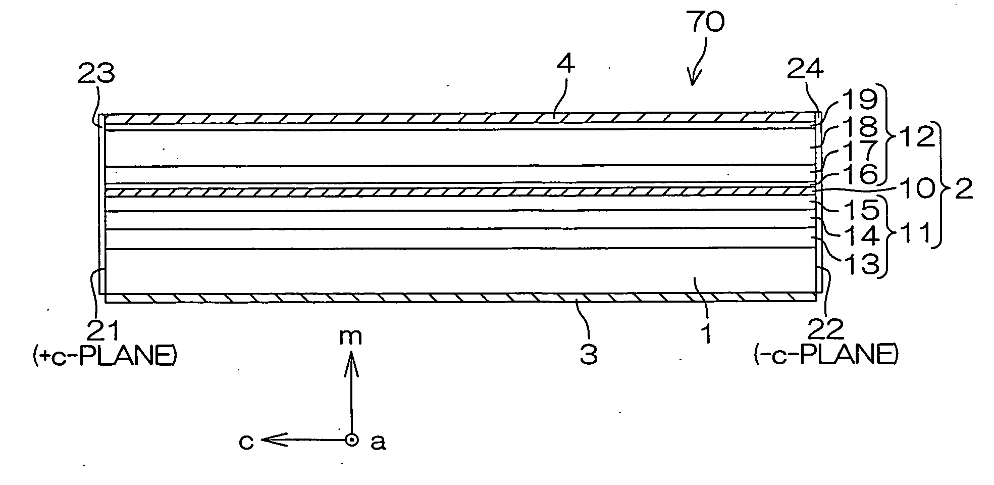
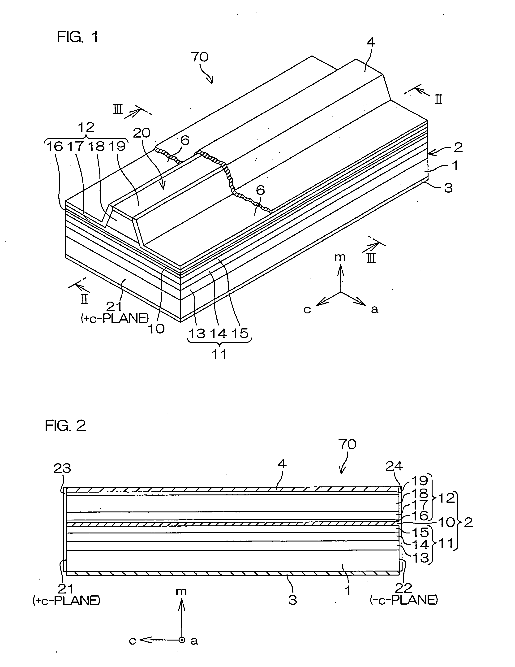
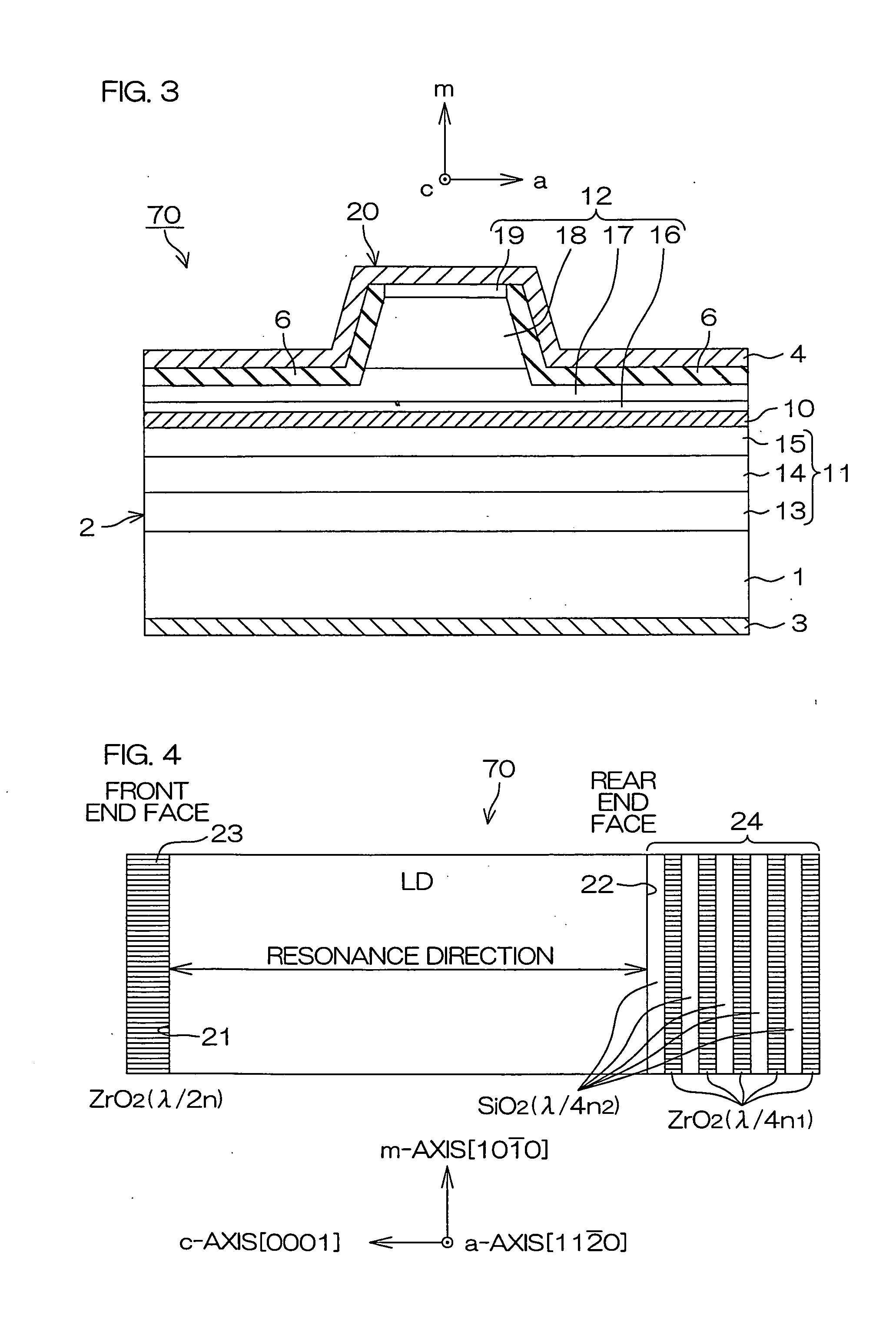
[0099]FIG. 9 is a perspective view showing the structure of a semiconductor laser diode according to the present invention, and FIG. 10 is a longitudinal sectional view along a line X-X in FIG. 9. Referring to FIGS. 9 and 10, portions corresponding to the respective portions shown in the aforementioned FIGS. 1 to 3 are denoted by the same reference numerals.
[0100]In a semiconductor laser diode 80 according to this embodiment, a ridge stripe 20 is formed parallelly to an a-axis direction, and hence both of cavity end faces 21 and 22 are defined by a-planes. The cavity end faces 21 and 22 are also defined by cleavage planes formed by cleavage.
first embodiment
[0101]Stacking faults resulting from epitaxy of a group III nitride semiconductor multilayer structure 2 are formed parallelly to a c-plane. In the structure of the aforementioned first embodiment, therefore, it follows that stacking faults and the waveguide intersect with one another. According to this embodiment, on the other hand, a stripe direction is rendered parallelized town a-axis, and hence a waveguide is parallel to the a-axis. The a-axis is parallel to a c-plane, whereby stacking faults formed parallelly to the c-plane do not intersect with the waveguide. Thus, disturbance of a light guide and increase in a leakage current resulting from stacking faults can be avoided.
third embodiment
[0102]FIG. 11 is a perspective view for illustrating the structure of a semiconductor laser diode according to the present invention. Referring to FIG. 11, portions corresponding to the respective portions shown in the aforementioned FIG. 1 are denoted by the same reference numerals.
[0103]In a semiconductor laser diode 90 according to this embodiment, a layer containing In including biaxial stress, i.e., an n-type InGaN Layer 26 (having a thickness of 0.1 μm, for example: the n-type impurity concentration is 1×1018 cm−3) is interposed between a substrate 1 and an n-type GaN contact layer 13 in a group III nitride semiconductor multilayer structure 2. The n-type InGaN layer 26 is provided so that the group III nitride semiconductor multilayer structure 2 can be inhibited from formation of cracks parallel to a c-plane due to the biaxial stress thereof.
[0104]When the substrate 1 is formed by a GaN single-crystalline substrate 1 having a major surface defined by an m-plane and the group...
PUM
 Abstract
Description
Claims
Application Information