Method for producing a bonded substrate

a technology of bonded substrates and substrates, applied in the direction of basic electric elements, electrical apparatus, semiconductor devices, etc., can solve the problems of high bonding strength, difficult etc., and achieve the effect of easy production of bonded substrates

Active Publication Date: 2010-12-02
SHIN ETSU CHEM IND CO LTD
View PDF8 Cites 3 Cited by
  • Summary
  • Abstract
  • Description
  • Claims
  • Application Information

AI Technical Summary

Benefits of technology

[0009]The present invention provides a method for producing a bonded substrate, the method being able to easily produce a bonded substrate comprising a SiGe film or Ge film (hereinafter, may also be referred to as a Si1-xGex film (wherein x is a number satisfying 0<x≦1)) in which a larger biaxial strain has been introduced than ever.

Problems solved by technology

However, since the strength of bonding between the donor and handle wafers is sufficiently high, the donor wafer is not allowed to expand in such a manner that the donor wafer is pulled by the handle wafer.
However, since the handle wafer has a thermal expansion coefficient lower than the donor wafer, the handle wafer hardly contracts.
The sufficiently high bonding strength as described above does not allow the Si1-xGex (01-xGex (0

Method used


Image

  • Method for producing a bonded substrate
  • Method for producing a bonded substrate

Examples


example

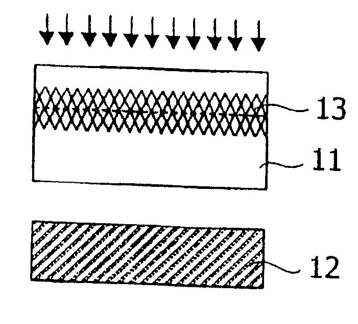
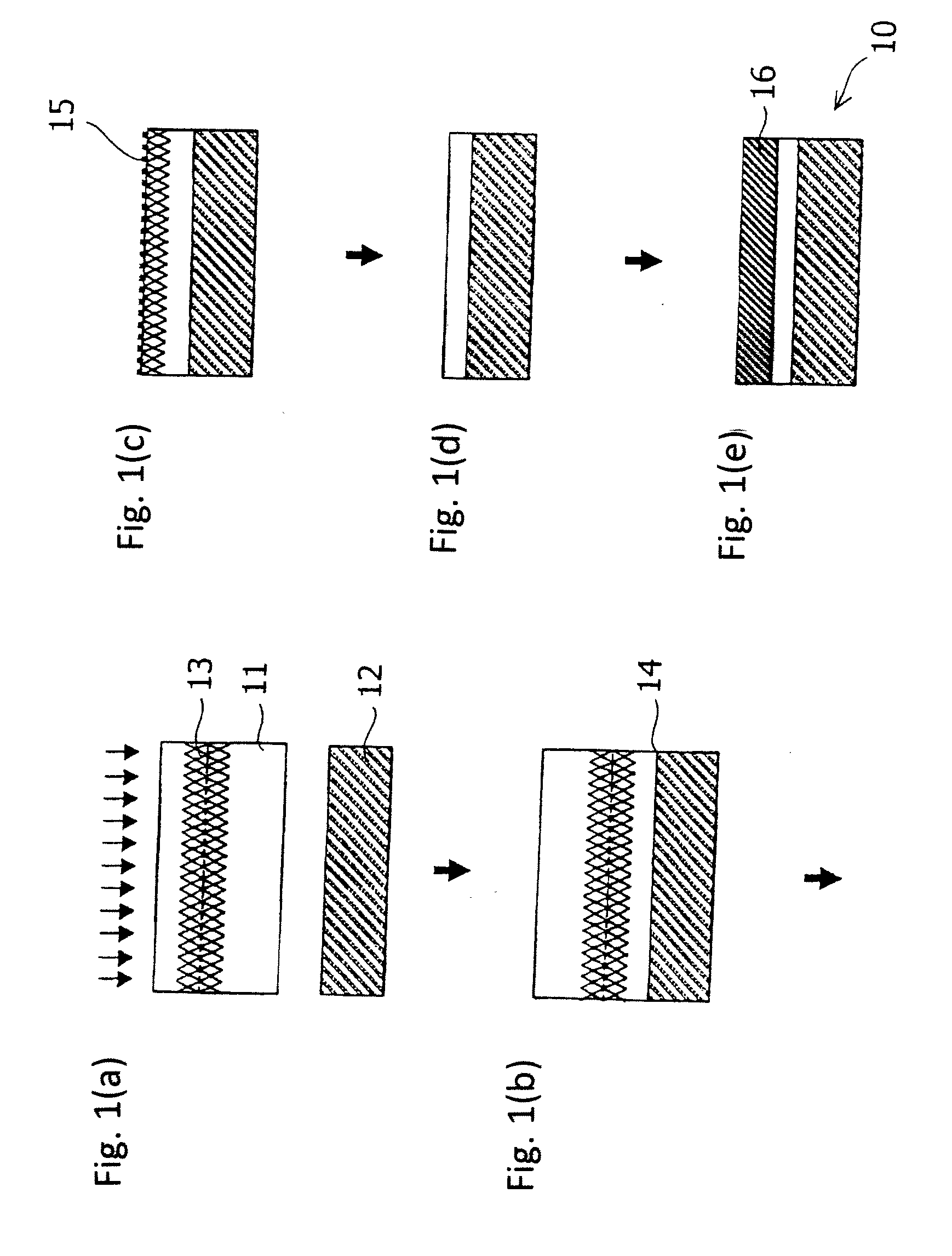
[0060]Thirty bonded substrates were produced as shown in FIG. 1 according to the method for producing a bonded substrate as follows.

[0061]First, a silicon substrate as a donor wafer and a quartz substrate as a handle wafer were provided. Next, hydrogen ions were implanted into one surface of the donor wafer to form a hydrogen-ion-implanted layer therein. As the ion implantation conditions, the implantation energy was 35 keV, the implantation dose was 9×10¹⁶ / cm2, and the implantation depth was 0.3 μm.

[0062]Next, the ion-implanted silicon substrate was placed in a plasma treatment apparatus. After nitrogen is introduced as a plasma gas therein, a high-frequency plasma treatment was performed for 10 seconds on the ion-implanted surface by applying a high frequency of 13.56 MHz between parallel plate electrodes each having a diameter of 300 mm under a reduced pressure condition of 2 Ton (270 Pa) and a high-frequency power condition of 50 W. In this manner, a surface activation treatment...


PUM


Abstract

A method for producing a bonded substrate having a Si1-xGex (0<x≦1) film in which a larger than ever biaxial strain has been introduced. Specifically, the method involves at least the steps of: providing a donor wafer and a handle wafer having a thermal expansion coefficient lower than the donor wafer, implanting ions of any one or both of hydrogen and a noble gas into the donor wafer to form an ion-implanted layer, performing a plasma activation treatment on at least one of bonding surfaces of the donor wafer and the handle wafer, bonding the donor wafer to the handle wafer, splitting the donor wafer through application of a mechanical impact to the ion-implanted layer, performing a surface treatment on a split surface of the donor wafer, and epitaxially growing a Si1-xGex (0<x≦1) film on the split surface to thus form a strained Si1-xGex (0<x≦1) film on the bonded wafers.

Description

BACKGROUND OF THE INVENTION[0001]1. Field of the Invention[0002]The present invention relates to a method for producing a bonded substrate. Particularly, the present invention relates to a method for producing a bonded substrate comprising a Si1-xGex (wherein x is a number satisfying 0<x≦1) film in which a biaxial strain has been introduced.[0003]2. Description of Related Art[0004]A strained silicon substrate in which a strain is induced in a silicon layer has been proposed in addition to a conventional bulk silicon wafer and silicon-on-insulator (SOI). The strained silicon substrate is one of means for increasing the carrier mobility in a semiconductor device.[0005]In a typical method for producing the strained silicon substrate, a SiGe layer containing 15% to 20% germanium (molar concentration) is epitaxially grown on a silicon wafer, and silicon is epitaxially grown on the SiGe layer to obtain a strained silicon layer (see, for example, R. People, “Physics and applications of ...

Claims


Application Information

Patent Timeline
Patent Type & Authority Applications(United States)
IPC IPC(8): H01L29/12H01L21/762
CPCH01L21/187H01L29/1054H01L21/76254
Inventor AKIYAMA, SHOJI
Owner SHIN ETSU CHEM IND CO LTD
Why Eureka
Try Eureka