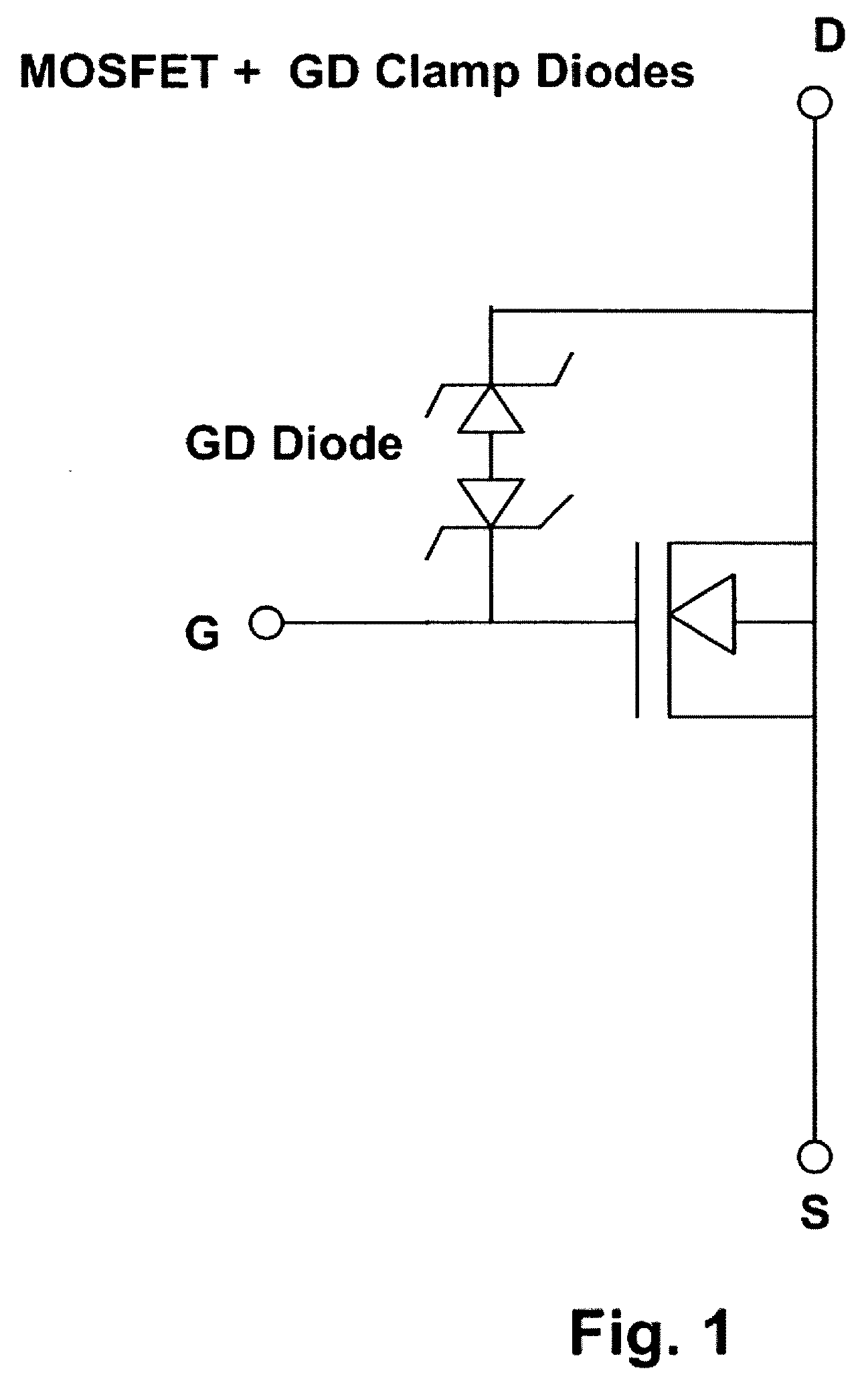
[0007]One
advantage of the present invention is that, gate-drain clamp diodes
and gate-source clamp diodes of MOSFET (or gate-collector clamp diodes
and gate-emitter clamp diodes of IGBT) share same gate
metal pad, as shown in FIG. 3A (or FIG. 3B for IGBT) of circuit Diagrams and FIG. 4 of top view. The first gate metal pad 550 in FIG. 4 located inside of the metal field plate ring area 552 is connected directly to
trench gate of MOSFET (IGBT) or through a
resistor (not shown). The first gate metal pad 550 is also connected to source metal 553 (or emitter metal for IGBT) through a gate-source clamp
diode 554 of MOSFET (or gate-emitter clamp
diode for IGBT) and the metal field plate 552 as gate metal runner as well. The second gate metal pad 551 located outside of edge termination including the metal field plate ring area 552 is connected to drain of MOSFET (or collector of IGBT) through a gate-drain clamp diode 555 (or gate-collector clamp diode for IGBT). The second gate metal pad is connected to the first gate metal pad through metal stripe with metal gap between two adjacent metal stripes, as shown in FIGS. 5A and 5B which is the C-D cross section view and E-F cross section view of FIG. 4, respectively. The metal gap 400 allows electrical field in the termination area out of epitaxial surface. There will be no degradation in breakdown voltage due to no polysilicon clamp diodes crossing over the edge termination.
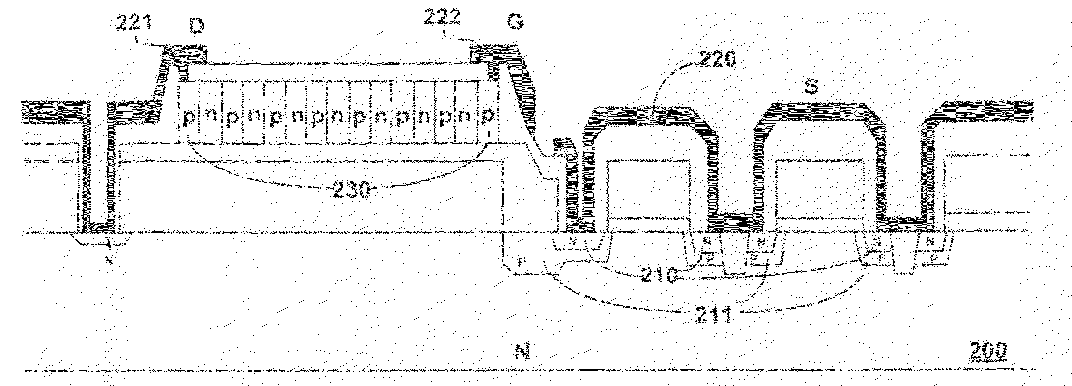
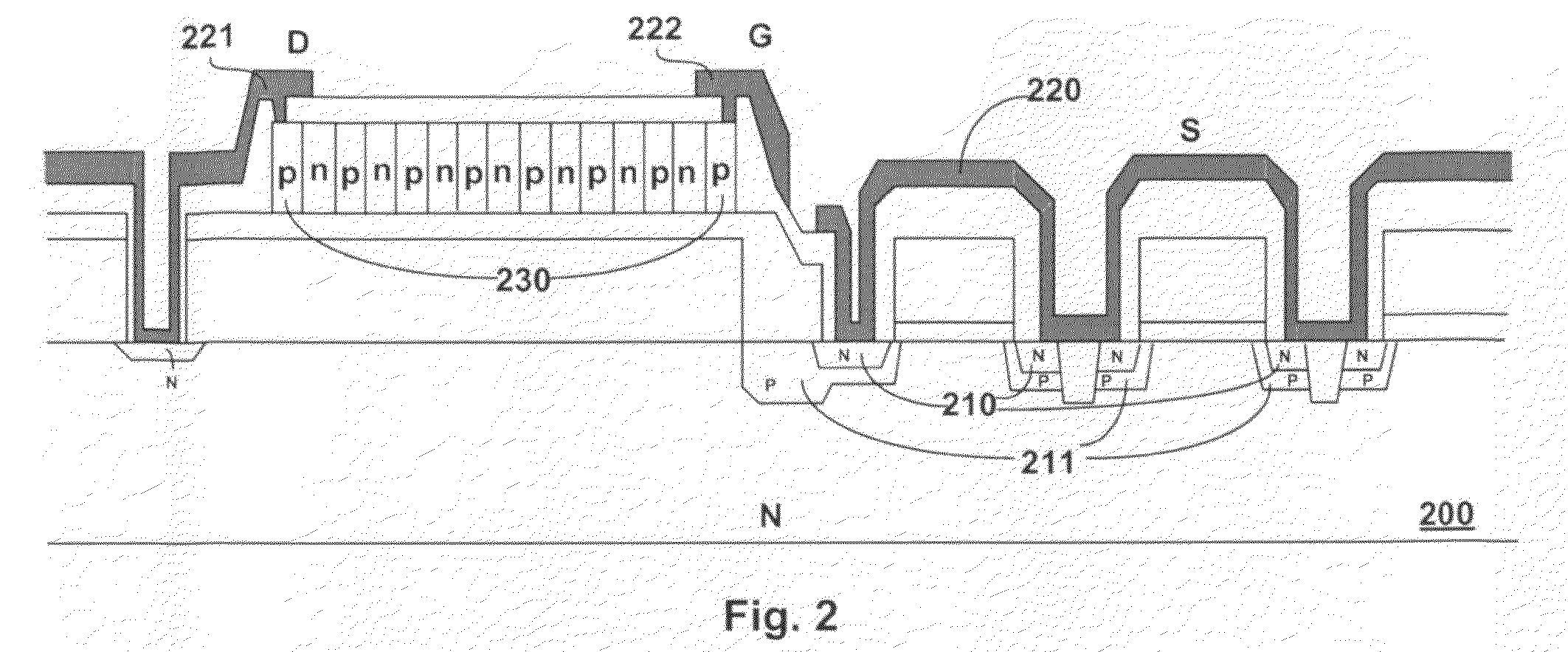
[0008]Briefly in a preferred embodiment according to the present invention, as shown in FIG. 6, which is also the A-B cross section view of FIG. 4, the present invention discloses a
trench MOSFET device formed on a substrate heavily doped with a first
semiconductor doping type, e.g., N+
doping type. Onto said substrate, grown an N epitaxial layer and a plurality of trenches were etched wherein. Doped poly was filled within a plurality of trenches over a
gate oxide layer along the inner surface of said trenches to serve as trench gates. Especially, the trench gates underneath contact trenches of gate-drain clamp diodes
and gate-source clamp diodes are employed to prevent shortage may caused by over
etching of contact trenches. Near the top surface of P-
body regions, N+ source regions are formed between two adjacent trench gates. A thick
oxide interlayer is deposited over epitaxial layer, as well as over the top surface and sidewalls of a doped polysilicon layer comprising multiple back to back Zener diodes which composed of alternated
doping areas of a first semiconductor doping type next to doping areas of a second semiconductor doping type. Through the thick
oxide interlayer, source-
body contact trenches, gate contact trenches and drain contact trenches are etched into epitaxial layer for source-body connection, gate connection and drain connection, respectively. Around the bottom of these contact trenches, a p+ contact area is formed. Especially, N+ contact regions are implanted near the bottom of the drain contacts trenches to further reduce the
contact resistance. Meanwhile, other contact trenches are etched into cathodes of the Zener diodes for the formation of gate-drain clamp diodes and gate-source clamp diodes. To fill these contact trenches, a
barrier layer and
tungsten material are deposited and then etched back to act as metal plug. The first gate metal pad 550 and the second gate metal pad 551 is deposited to contact one
electrode of gate-source clamp diodes and gate-drain clamp diodes via trench contacts etched into Zener diodes, respectively. At the same time, source metal is deposited to contact another
electrode of gate-source clamp diodes with source region and
body regions; drain metal is deposited to contact the other
electrode of gate-drain clamp diodes with drain region. In termination area, gate metal runner which also serving as metal field plate is formed overlying P-body and top surface of epitaxial layer which connects both two said gate metal pads together. The gate-drain clamp diode as shown in FIG. 6 is located outside of termination and has no gate metal or polysilicon
cross over the edge termination, therefore resulting in no degradation in breakdown voltage which occurred in the prior art.
[0009]Briefly in another preferred embodiment according to the present invention, as shown in FIG. 7, which also shows the A-B cross section view of FIG. 4, the
trench MOSFET structure disclosed is similar to the structure in FIG. 6 except that there is a deep
guard ring under said metal field plate in termination area.
[0010]Briefly in another preferred embodiment according to the present invention, as shown in FIG. 8, which also shows the A-B cross section view of FIG. 4, the
trench MOSFET structure disclosed is similar to the structure in FIG. 6 except that there are n* regions in top surface of said epitaxial layer next to P-
body region as termination and there are n* regions having higher doping concentration than the epitaxial layer underneath trench bottom for Rds reduction.
[0011]Briefly in another preferred embodiment according to the present invention, as shown in FIG. 9, which also shows the A-B cross section view of FIG. 4, the trench MOSFET structure disclosed is similar to the structure in FIG. 8 except that there is a deep
guard ring under said metal field plate in termination area.
[0012]Briefly in a preferred embodiment according to the present invention, as shown in FIG. 10, which is also the A-B cross section view of FIG. 4. The present invention discloses a
trench IGBT device formed on a substrate heavily doped with a second semiconductor doping type, e.g., P+ doping type. Onto said substrate, grown a heavily doped epitaxial layer with a first semiconductor doping type, e.g., N+ doping type, onto which a second epitaxial layer lightly doped with the same first doping type is formed, and a plurality of trenches were etched wherein. Doped poly was filled within a plurality of trenches over a
gate oxide layer along the inner surface of said trenches to serve as trench gates. Especially, the trench gates underneath contact trenches of gate-collector clamp diodes and gate-emitter clamp diodes are employed to prevent shortage may caused by over
etching of contact trenches. Near the top surface of P-
body regions, N+ emitter regions are formed between two adjacent trench gates. A thick
oxide interlayer is deposited over front surface of epitaxial layer, as well as over the top surface and sidewalls of doped polysilicon layer comprising multiple back to back Zener diodes which composed of alternated doping areas of a first semiconductor doping type next to doping areas of a second semiconductor doping type. Through the thick oxide interlayer, emitter-base contact trenches, gate contact trenches and collector contact trenches are etched into the second epitaxial layer for emitter-base connection, gate connection and collector connection, respectively. Around the bottom of these contact trenches, a p+ contact area is formed. Especially, N+ contact regions are implanted near the bottom of the collector contacts trenches to further reduce the
contact resistance. Meanwhile, other contact trenches are etched into cathodes of the Zener diodes for the formation of gate-collector clamp diodes and gate-emitter clamp diodes. To fill these contact trenches, a
barrier layer and
tungsten material are deposited and then etched back to act as metal plug. The first gate metal pad and the second gate metal pad is deposited to contact one electrode of gate-collector clamp diodes and gate-emitter clamp diodes via trench contacts etched into Zener diodes, respectively. At the same time, emitter metal is deposited to contact another electrode of gate-emitter clamp diodes with emitter region and base regions; collector metal is deposited to contact the other electrode of gate-collector clamp diodes with collector region. In termination area, gate metal runner which also serving as metal field plate is formed overlying P-body and top surface of epitaxial layer which connects both two said gate metal pads together and there is a deep
guard ring and a floating ring under said metal field plate under said metal field plate as termination.

