Integrated Direct Conversion Detector Module

a detector module and direct conversion technology, applied in the field of electronic imaging systems, can solve problems such as noise and added interconnection complexity

Inactive Publication Date: 2010-12-30
GENERAL ELECTRIC CO
View PDF6 Cites 29 Cited by
  • Summary
  • Abstract
  • Description
  • Claims
  • Application Information

AI Technical Summary

Benefits of technology

[0011]In still another aspect of the present invention, a method of fabricating an imaging sensor array comprises: providing a plurality of imaging modules, each imaging module fabricated from a direct conversion crystal having a redistribution layer for attaching a readout integrated circuit to an anode layer on the direct

Problems solved by technology

However, such conventional configurations introduces noise and added interconnect complexity because of

Method used


Image

  • Integrated Direct Conversion Detector Module
  • Integrated Direct Conversion Detector Module
  • Integrated Direct Conversion Detector Module

Examples


Embodiment Construction

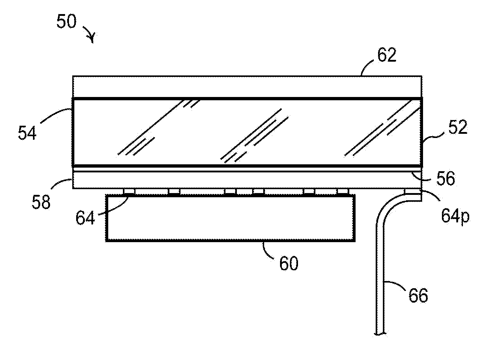
[0030]The present invention provides for an imaging module having an interposer, or redistribution layer, created on the pixel side of a direct conversion crystal. This design serves to adapt a crystal pad array layout to that of a lead configuration on a readout integrated circuit. The redistribution layer provides for an optimized imaging module design with minimum interconnect complexity and low capacitance, reducing noise propagation by directly attaching the readout integrated circuit to the backside of the direct conversion crystal. The resulting imaging module component can be used as an individual sensor array, or may be tiled with other imaging modules to create a sensor array having a much greater imaging surface than an individual imaging module.

[0031]Referring now to FIG. 4, a diagrammatical edge view illustrating a stack up of an imaging module 50, in accordance with one aspect of the present invention. The imaging module 50 comprises a direct conversion crystal 52 for ...


PUM


Abstract

A detector module comprises: a direct conversion crystal for converting incident photons into electrical signals, the direct conversion crystal having an anode layer deposited on a first surface and a cathode layer deposited on a second surface; a redistribution layer deposited on the anode layer, the redistribution layer configured to adapt a pad array layout of the direct conversion crystal to a predetermined lead pattern; an integrated circuit in electrical communication with the direct conversion crystal; and a plurality of input/output electrical paths connected to the redistribution layer to provide connectivity between the imaging module and another level of interconnect.

Description

BACKGROUND OF THE INVENTION[0001]The subject matter disclosed herein relates to electronic imaging systems and, more particularly, to modular imaging sensor arrays.[0002]X-ray and computed tomography imaging systems have been utilized for observing interior aspects of a patient or objects of interest. A detecting device is typically positioned to detect radiation attenuated from passing through the patient or object. There is shown in the isometric diagrammatical illustration of FIG. 1 a “third generation” CT imaging system 10 configured to perform computed tomography imaging on a patient 22 by means of photon counting and energy discrimination of x-rays at high flux rates, as is known in the relevant art. The CT imaging system 10 comprises a gantry 12, with a collimator assembly 18, a data acquisition system 32, and an x-ray source 14 disposed on the gantry 12 as shown.[0003]Operation of the CT imaging system 10 may be described with reference to the functional block diagram of FIG...

Claims


Application Information

Patent Timeline
IPC IPC(8): G01T1/24H01L21/50
CPCH01L23/3677H01L23/42H01L2924/1532H01L24/48H01L25/16H01L27/14618H01L2224/48091H01L2224/48227H01L2224/73253H01L2924/01078H01L2924/01079H01L2924/14H01L2924/15311H01L2924/00014H01L2224/45099H01L2224/45015H01L2924/207
Inventor WOYCHIK, CHARLES GERARDROSE, JAMESTKACZYK, JOHN ERICSHORT, JONATHANDU, YANFENG
Owner GENERAL ELECTRIC CO
Why Eureka
Try Eureka