Semiconductor device and method of manufacturing the same

a technology of semiconductor devices and semiconductors, applied in semiconductor devices, semiconductor/solid-state device details, electrical apparatus, etc., can solve problems such as unnecessary gate negative power sources

Inactive Publication Date: 2010-12-30
RENESAS ELECTRONICS CORP
View PDF1 Cites 27 Cited by
  • Summary
  • Abstract
  • Description
  • Claims
  • Application Information

AI Technical Summary

Benefits of technology

[0021]That is, in the semiconductor device having the silicon-based plug extending through the boundary surface between the first and second semiconductor layers having different impurity concentrations such as the boundary surface between the silicon-based mono-crystalline substrate layer and the epitaxial substrate, at least the inside of the plug is a poly-crystalline region, and the portions of the surface of the poly-crystalline region located on both sides of the foregoing boundary surface in adjacent relation thereto are covered with the solid-phase epitaxial region so that an undesired stress does not occur around the plug.

Problems solved by technology

Moreover, since the LDMOSFET can operate in a class AB mode, a gate negative power source and the like are unnecessary.

Method used


Image

  • Semiconductor device and method of manufacturing the same
  • Semiconductor device and method of manufacturing the same
  • Semiconductor device and method of manufacturing the same

Examples


Embodiment Construction

Outline of Embodiments

[0048]First, a description will be given of the outline of representative embodiments of the invention disclosed in the present application.

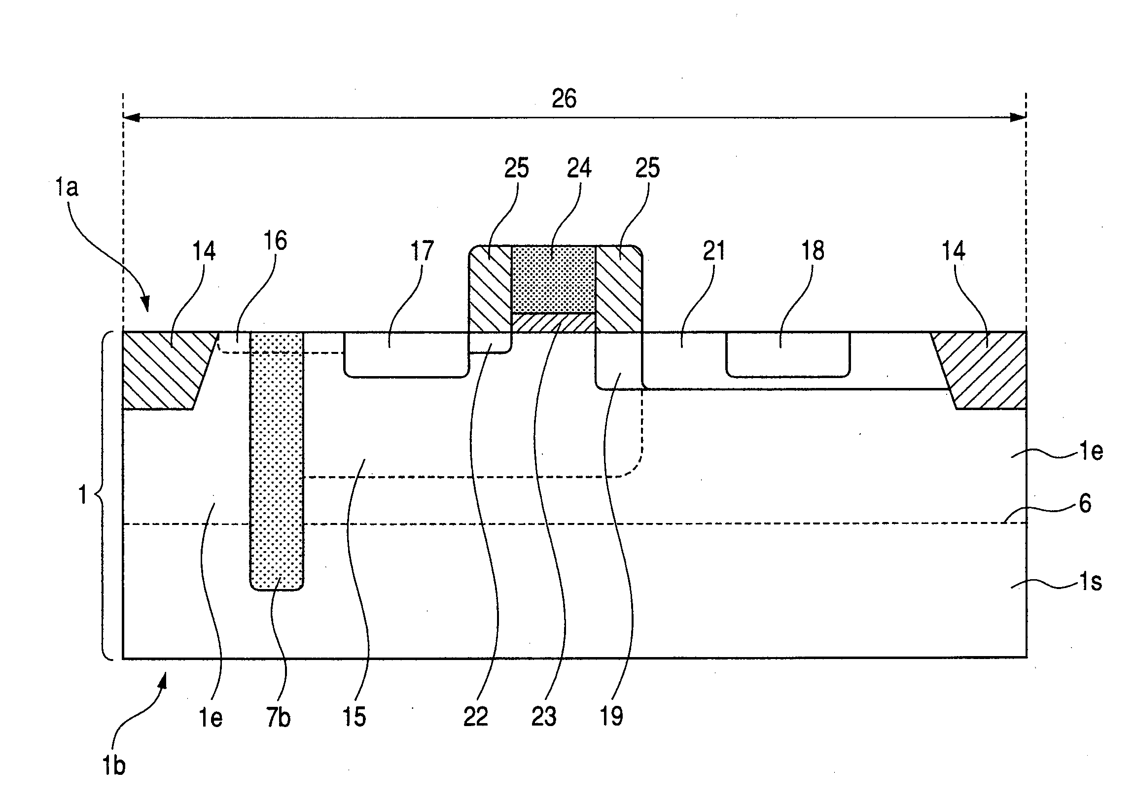
[0049]1. A semiconductor device includes: (a) a semiconductor substrate comprised of a silicon-based single crystal of a first conductivity type, and having a first main surface and a second main surface; (b) a first semiconductor layer provided closer to the second main surface in the semiconductor substrate, and having a first impurity concentration; (c) a second semiconductor layer provided closer to the first main surface in the semiconductor substrate so as to come in contact with the first semiconductor layer, and having a second impurity concentration; and (d) a silicon-based plug extending from the first main surface through the second semiconductor layer to reach an inside of the first semiconductor layer, wherein the plug includes: (d1) a poly-crystalline region in a center portion thereof; and (d2) a solid-phase ...


PUM


Abstract

In a semiconductor device having an LDMOSFET, a source electrode is at the back surface thereof. Therefore, to reduce electric resistance between a source contact region in the top surface and the source electrode at the back surface, a poly-silicon buried plug is provided which extends from the upper surface into a P+-type substrate through a P-type epitaxial layer, and is heavily doped with boron. Dislocation occurs in a mono-crystalline silicon region around the poly-silicon buried plug to induce a leakage failure. The semiconductor device has a silicon-based plug extending through the boundary surface between first and second semiconductor layers having different impurity concentrations. At least the inside of the plug is a poly-crystalline region. Of the surface of the poly-crystalline region, the portions located on both sides of the foregoing boundary surface in adjacent relation thereto are each covered with a solid-phase epitaxial region.

Description

CROSS-REFERENCE TO RELATED APPLICATIONS[0001]The disclosure of Japanese Patent Application No. 2009-153254 filed on Jun. 29, 2009 including the specification, drawings and abstract is incorporated herein by reference in its entirety.BACKGROUND OF THE INVENTION[0002]The present invention relates to a technology which is effective when applied to a technique for burying a plug in a silicon-based semiconductor substrate in a structure of a semiconductor device (or a semiconductor integrated circuit device) and a method of manufacturing the same.[0003]In Japanese Unexamined Patent Publication No. 2007-053124 (Patent Document 1), disclosed is a technology for an integrated circuit including a Laterally Diffused Metal Oxide Semiconductor Field Effect Transistor (LDMOSFET) in which a silicon-based buried plug of poly-silicon or the like is formed in a silicon-based mono-crystalline semiconductor substrate.[0004]In Japanese Unexamined Patent Publication No. 2004-103715 (Patent Document 2), ...

Claims


Application Information

Patent Timeline
Patent Type & Authority Applications(United States)
IPC IPC(8): H01L29/78H01L21/768
CPCH01L21/02057H01L21/743H01L29/4175H01L29/66659H01L2924/0002H01L29/7835H01L2924/00
Inventor ARIE, HIROYUKIUMEMURA, NOBUAKIHATTORI, NOBUYOSHINAKANISHI, NOBUTOHARA, KIMIONITTA, KYOYAISHIKAWA, MAKOTO
Owner RENESAS ELECTRONICS CORP
Why Eureka
Try Eureka