Laminated ceramic electronic component and manufacturing method therefor

a technology of laminated ceramics and electronic components, applied in the direction of fixed capacitor details, stacked capacitors, fixed capacitors, etc., can solve the problems of structural defects, defects in reliability, and other moisture likely to enter the component main body along the interface between the internal electrodes and the ceramic layer

a technology of laminated ceramics and electronic components, applied in the direction of fixed capacitor details, stacked capacitors, fixed capacitors, etc., can solve the problems of structural defects, defects in reliability, and other moisture likely to enter the component main body along the interface between the internal electrodes and the ceramic layer

US20100328843A1Active Publication Date: 2010-12-30MURATA MFG CO LTD

Image

  • Laminated ceramic electronic component and manufacturing method therefor
  • Laminated ceramic electronic component and manufacturing method therefor
  • Laminated ceramic electronic component and manufacturing method therefor

Examples


Embodiment Construction

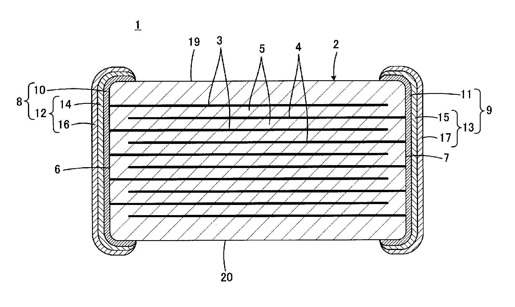
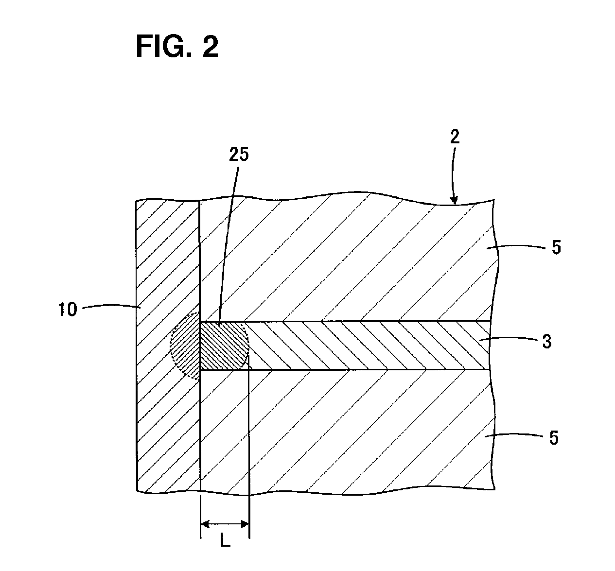
[0027]A laminated ceramic electronic component 1 according to a preferred embodiment of the present invention and a manufacturing method therefor will be described with reference to FIGS. 1 and 2.

[0028]A laminated ceramic electronic component 1 includes a component main body 2 having a laminated structure. The component main body 2 includes a plurality of internal electrodes 3 and 4 therein. More specifically, the component main body 2 includes a plurality of laminated ceramic layers 5, and a plurality of layered internal electrodes 3 and 4 arranged at interfaces between the adjacent ceramic layers 5. The internal electrodes 3 and 4 preferably primarily include nickel, for example.

[0029]When the laminated ceramic electronic component 1 is a laminated ceramic capacitor, the ceramic layers 5 are preferably made of a dielectric ceramic. It is to be noted that the laminated ceramic electronic component 1 may define a different element such as an inductor, a thermistor, or a piezoelectri...


PUM

PropertyMeasurementUnit
temperatureaaaaaaaaaa

Abstract

In a method for manufacturing a laminated ceramic electronic component, after a plating layer for an external terminal electrode is formed by applying copper plating to an end surface of a component main body at which respective ends of a plurality of internal electrodes primarily including nickel are exposed, when a heat treatment at a temperature of about 800° C. or more is applied in order to improve adhesion strength and resistance to moisture of the external terminal electrode, voids may occur in the plating layer. The step of applying a heat treatment at a temperature of about 800° C. or more to a component main body with plating layers formed thereon includes not only a step of maintaining a top temperature of about 1000° C. or more but also a step of maintaining a temperature of about 600° C. to 900° C. at least once before the step of maintaining the top temperature. These steps preliminarily diffuse copper included in the plating layers, which has a relatively high diffusion velocity, into the internal electrodes primarily including nickel, thereby reducing a difference in diffusion velocity between copper and nickel at the top temperature, which causes the occurrence of voids.

Description

BACKGROUND OF THE INVENTION[0001]1. Field of the Invention[0002]The present invention relates to a laminated ceramic electronic component and a method for manufacturing the laminated ceramic electronic component, and more particularly, to a laminated ceramic electronic component with external terminal electrodes formed directly by plating so as to be electrically connected to a plurality of internal electrodes, and a method for manufacturing the laminated ceramic electronic component.[0003]2. Description of the Related Art[0004]As shown in FIG. 4, a laminated ceramic electronic component 101 typified by a laminated ceramic capacitor generally includes a component main body 105 having a laminated structure, which includes a plurality of laminated ceramic layers 102 made of, for example, a dielectric ceramic, and a plurality of layered internal electrodes 103 and 104 arranged at interfaces between the adjacent ceramic layers 102. Respective ends of the plurality of internal electrodes...

Claims


Application Information

Patent Timeline
30 Dec 2010
Publication
US20100328843A1
IPC
H01G4/008; B05D5/12; H10N30/50
CPC
H01L41/293; H01G4/2325; Y10T29/435; H01L41/083; H01G4/30; H10N30/50; H10N30/063
Inventors
SARUBAN, MASAHITO; OGAWA, MAKOTO