

CMOS microelectromechanical system (MEMS) device and fabrication method thereof
a microelectromechanical and microelectromechanical technology, applied in the direction of fluid pressure measurement, fluid pressure measurement by electric/magnetic elements, instruments, etc., can solve the problems of defect of the mems device, undercutting of the interface between the silicon oxide and the silicon substrate, and damage to the mems structure, etc., to reduce the damage to the diaphragm and reduce the undercut
- Summary
- Abstract
- Description
- Claims
- Application Information
AI Technical Summary
Benefits of technology
Problems solved by technology
Method used
Image

Examples
Embodiment Construction
[0037]Several embodiments are provided for describing the invention but not for limiting the invention. Further, the embodiments can be properly combined to each other without limited to individual embodiments.
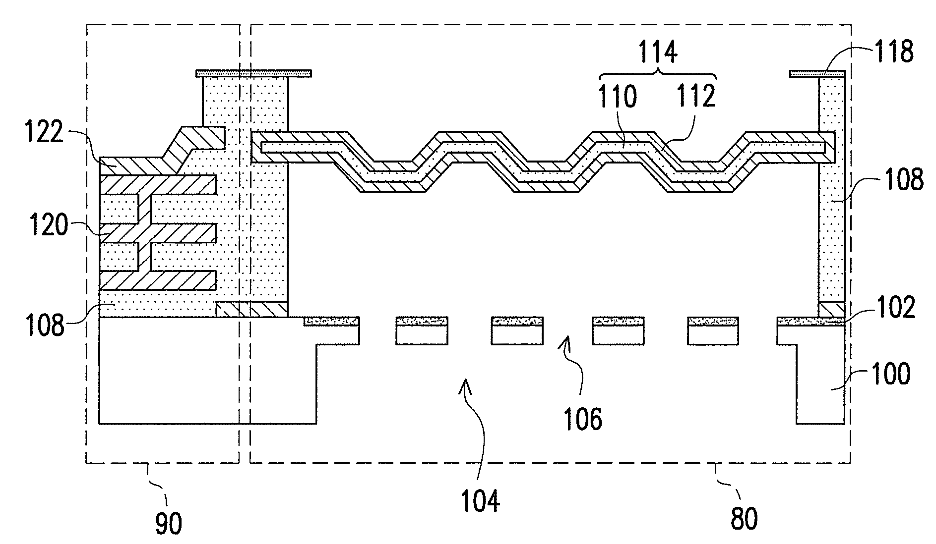
[0038]FIG. 3 is a cross-sectional view, schematically illustrating a MEMS device, according to an embodiment of the invention. In FIG. 3, the CMOS MEMS device includes the CMOS circuit 90 and MEMS device 80, which are fabricated over the same substrate 100. The CMOS circuit 90 is fabricated by usual semiconductor fabricating process to form the circuit 120 with the bonding pad 122, for example. The circuit 120 is embedded in the dielectric layer 108, and is also referred as the structural dielectric layer 108 in the invention. The circuit 120 is a part the whole CMOS circuit, in which just the interconnection is shown. The structural dielectric layer 108 includes some device structure or interconnecting having been embedded in the dielectric. The MEMS device 80 includes a diap...
PUM
 Abstract
Description
Claims
Application Information