Semiconductor differential amplifier

a technology of differential amplifier and semiconductor, applied in differential amplifiers, amplifiers with semiconductor devices/discharge tubes, amplifier details, etc., can solve the problem of limited feedback voltage range, achieve high gain operation, reduce the number of stacked transistors, and maximize output amplitude

Inactive Publication Date: 2011-01-06
NAT INST OF ADVANCED IND SCI & TECH
View PDF6 Cites 7 Cited by
  • Summary
  • Abstract
  • Description
  • Claims
  • Application Information

AI Technical Summary

Benefits of technology

[0020]By using this semiconductor differential amplifier, an differential input in a entire range from a power supply potential to the ground potential becomes acceptable. Even if a common-mode input level nearly equal to 0V, where the devices are turned to the off state, is input, the input common-mode signal detection circuit operates properly to turn the input transistor of the differential pair to the on state, and by modulating the on state with a differential input applied to the first gates, the differential pair can be operated normally.
[0021]Furthermore, since in the input transistor of the differential pair, an effect to reject the common-mode component and to maintain an output common-mode level can be obtained, as automatically adjusting the threshold voltage. Accordingly, tail current source, often used as a general differential pair becomes unnecessary, and number of stacked transistors can be reduced. As a result, the output amplitude can be maximized.
[0022]Furthermore, by designing the main body of the differential pair and the input common-mode signal detection circuit especially in accordance with the embodiments disclosed in the present description, each of the transistors in the differential pair can be operated in the saturation region, so that the differential pair realizes a high gain operation in any time.
[0023]In addition, even when the rejection of the common-mode component is not capable in the input transistors of the differential pair, the effect of the common-mode feedback performed in the current source load enables to reject the common-mode component and to suppress variation of the output common-mode level. In other words, an operation of the differential amplification can be realized more reliably.
[0024]The above circuit functions enable to ensure the input common-mode range and to maximize the output signal amplitude, both of which are necessary at the same time when the threshold voltage can not be scaled in accordance with the scaling of the power supply voltage. In addition, the circuit function is also effective when extremely decreasing the power supply voltage.
[0025]Furthermore, the above circuit functions can be realized with the four-terminal fin type FET, a fin type FET device of which two gates are separated. Therefore, in an integrated circuit using the four-terminal fin type FET enables to realize integration of a low power consumption digital circuit along with an analog circuit on the same substrate at low cost by utilizing the present invention.

Problems solved by technology

Also in this method, a range of the feedback voltage is limited.

Method used


Image

  • Semiconductor differential amplifier
  • Semiconductor differential amplifier
  • Semiconductor differential amplifier

Examples


first embodiment

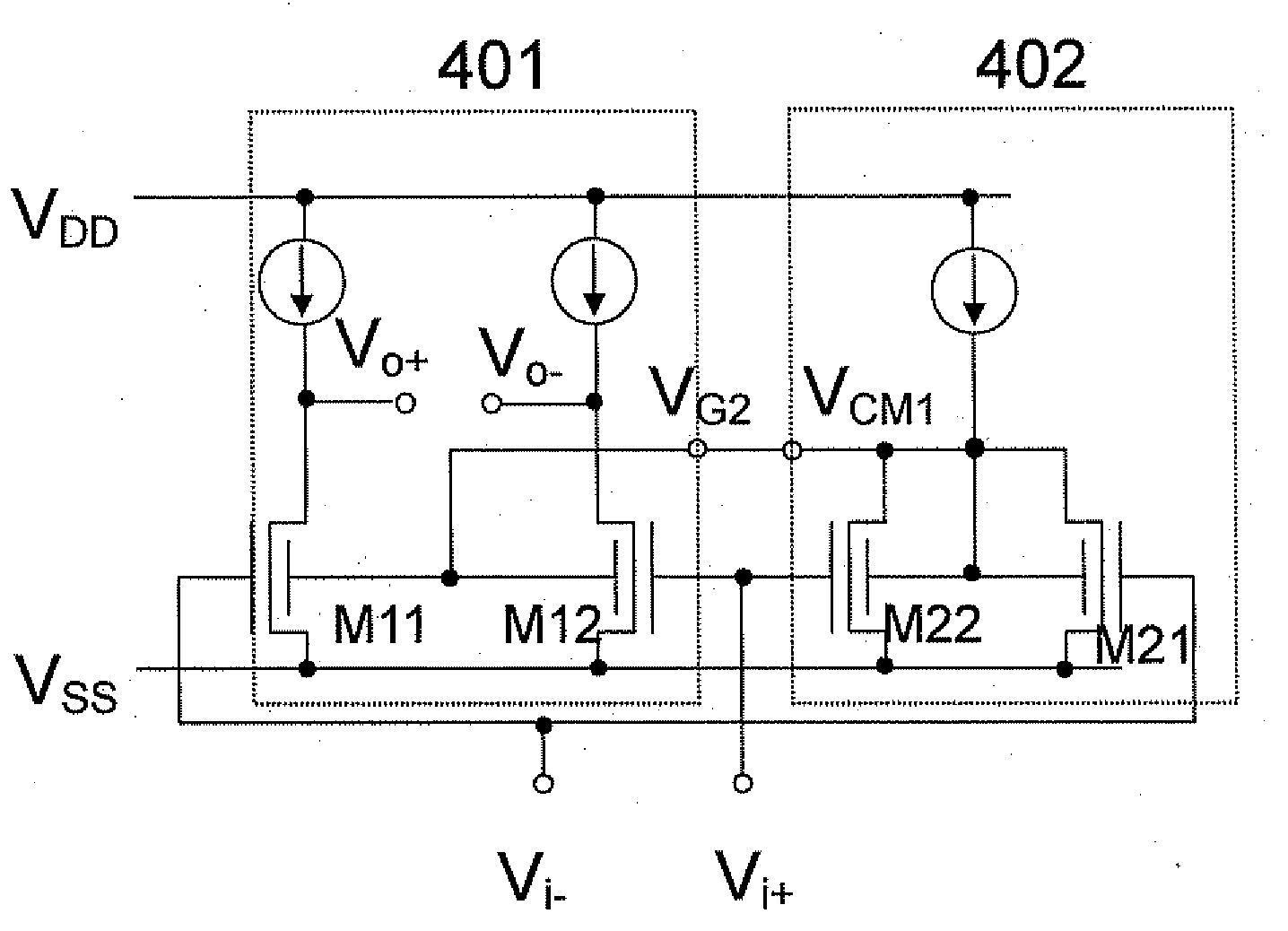
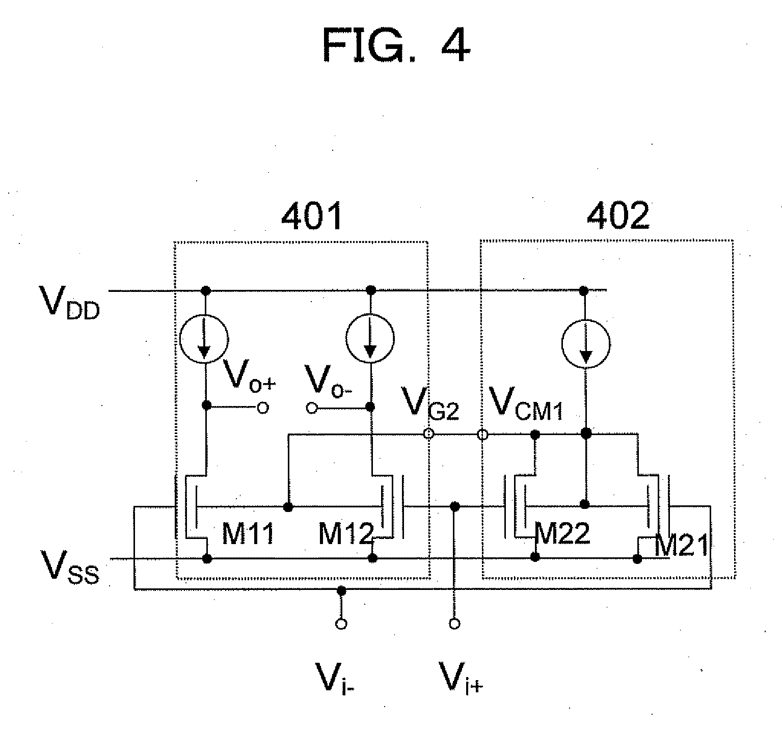
[0036]FIG. 4 shows the most fundamental circuit configuration disclosed in the present invention. In FIG. 4, numeral reference 401 denotes a main body of a differential pair, and 402 denotes an input common-mode component detection circuit. The most fundamental semiconductor differential amplifier is configured by inputting an output voltage VCM1 of the input common-mode signal detection circuit to a terminal VG2 of the differential pair 401.

[0037]Here, n-channel four-terminal fin type FETs M11, M12, M21, and M22 have a device structure as shown by 501 in FIG. 5. Symbols in a circuit diagram of M11, M12, M21 and M22 are shown by 502. These devices are fabricated by separating the usual connected gates of a typical fin type FET into a first gate 503 and a second gate 504. In this description, an input signal is input into the first gate and a signal for controlling the threshold voltage is input into the second gate.

[0038]In FIG. 5, 502 and 511 denote symbols showing an n-channel fou...

second embodiment

[0041]FIG. 6 shows the first embodiment for realizing a current source loads of the input common-mode signal detection circuit 402 and the main body of the differential pair 401 by p-type three-terminal fin type FETs M31, M32 and M4 which are realized by applying a common reference voltage to these p-channel three-terminal fin type FETs in details. However in this embodiment, when an input common-mode signal VCMi becomes too large, VCM1 approaches the ground potential, where the operation for common-mode rejection by M11 and M12 becomes impossible, and M11, M12 start to operate in a linear region.

third embodiment

[0042]A method to solve this problem is shown in FIG. 7. That is, to gates of p-channel four-terminal fin type FETs M31 and M32, a common-mode feedback signal VCM3 generated by n-channel three-terminal fin type FETs M51, M52 and M53 are input. Therefore, even when the common-mode rejection by M11, M12, M21 and M22 can not be performed, an operation in the saturation region is maintained, and the output common-mode level is kept constant in the main body of the differential pair 401.


PUM


Abstract

There is provided a circuit to make a bias for adjusting a threshold voltage of MOS devices available in a wide range, to extend the amplitude range of the input voltage range of a semiconductor differential amplifier from a power supply potential to a ground potential, and automatically to ensure an operation of a differential pair in the saturation region as rejecting the common-mode signal in the entire voltage range. The semiconductor differential amplifier is configured by the first gates of two four-terminal fin type FETs serving as an input terminal of differential pair, and in that the second gates of the four-terminal fin type FETs interconnected with each other, wherein a signal decreasing monotonously along with the increase in the input common-mode component is input.

Description

TECHNICAL FIELD[0001]The present invention relates to a semiconductor differential amplifier.BACKGROUND ART[0002]Semiconductor amplifiers are widely used for amplification of analog signals. In particular, a semiconductor differential amplifier is basically configured by a differential pair 102 including a current source 101 as shown in FIG. 1.[0003]Due to development of the CMOS (Complementary Metal Oxide-Semiconductor) integrated circuit technology, both digital circuits and analog circuits become to be integrated on the same substrate as used for the CMOS integrated circuit. Integration of various types of circuits on a single substrate enables miniaturization of the system and reduction in cost of the products.[0004]Such a development in integrated circuits has been achieved by size reduction of devices. The size reduction of devices leads to improvement of the circuit performance, especially of the digital circuit which is a main part of the integrated circuit. In other words, ...

Claims


Application Information

Patent Timeline
Patent Type & Authority Applications(United States)
IPC IPC(8): H03F3/45
CPCH03F3/45183H03F2203/45354H03F2203/45342H03F1/0261
Inventor OUCHI, SHINICHI
Owner NAT INST OF ADVANCED IND SCI & TECH
Why Eureka
Try Eureka