Semiconductor component with trench insulation and corresponding production method

a technology of semiconductors and components, applied in the direction of semiconductor devices, basic electric elements, electrical appliances, etc., can solve the problems of undesirable leakage currents, insufficient conventional trench isolation, and no longer suitable conventional locos methods, so as to reduce the area requirement and improve the integration density

Active Publication Date: 2011-01-06
INFINEON TECH AG
View PDF17 Cites 6 Cited by
  • Summary
  • Abstract
  • Description
  • Claims
  • Application Information

AI Technical Summary

Benefits of technology

[0008]Therefore, the invention is based on the object of providing a semiconductor component with trench isolation and an associated fabrication m

Problems solved by technology

As the integration density rises, however, such conventional LOCOS methods are no longer suitable since they have a high area requirement.
Nevertheless, such a conventional trench isolation is also often insufficient since so-called punch-through effects occur in the semiconductor material.
Undesirable leakage currents are observed

Method used


Image

  • Semiconductor component with trench insulation and corresponding production method
  • Semiconductor component with trench insulation and corresponding production method
  • Semiconductor component with trench insulation and corresponding production method

Examples


first exemplary embodiment

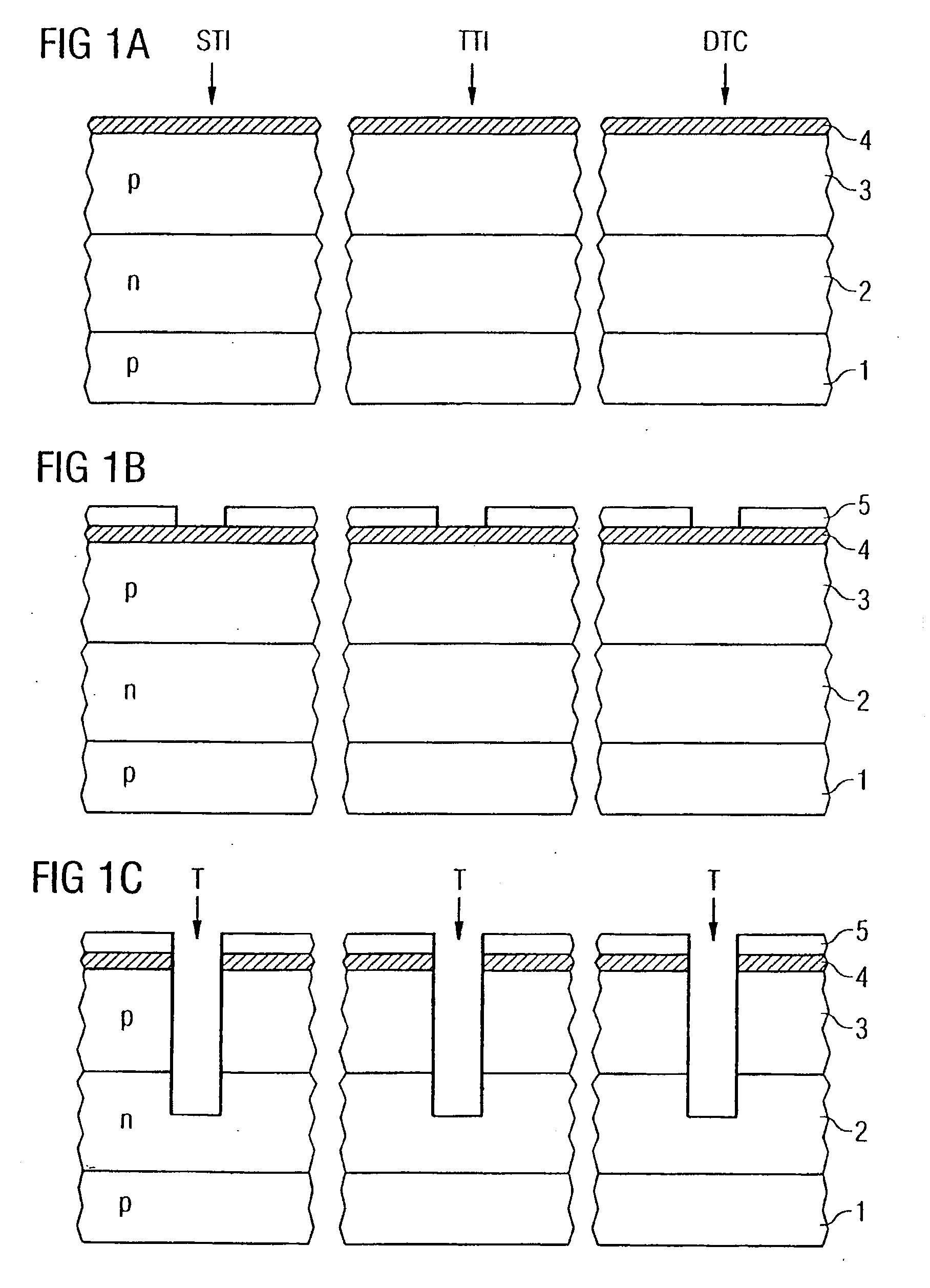
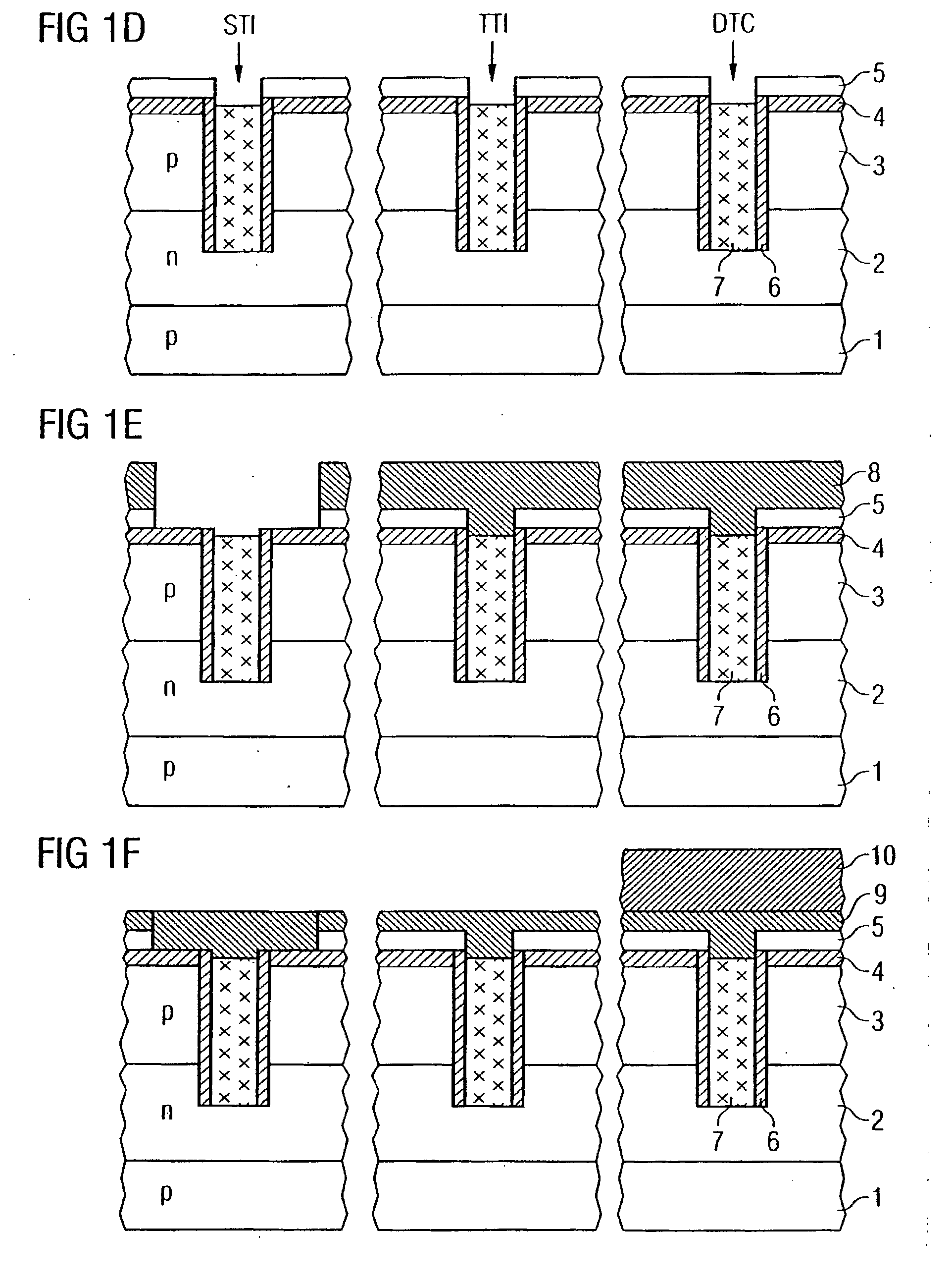
[0024]FIGS. 1A to 1N show simplified sectional views of a semiconductor component with a—in an upper region—widened but shallow trench isolation STI, a—in its upper region—thin trench isolation TTI and an associated trench contact DTC (Deep Trench Contact) in accordance with a first exemplary embodiment.

[0025]In accordance with FIG. 1A, firstly different doping regions are formed in a common carrier material such as e.g. a semiconductor substrate, the reference symbol 1 for example representing a p-type semiconductor substrate or a deep p-type well, the reference symbol 2 an n-type well and the reference symbol 3 a (shallow) p-type well. The wells or doping regions 1, 2 and 3 may be formed for example by means of ion implantation or other doping methods, silicon preferably being used as semiconductor material.

[0026]By way of example, a first insulation layer 4 in the form of an oxide layer is deposited or grown at the surface of the semiconductor substrate. A double or triple well s...

second exemplary embodiment

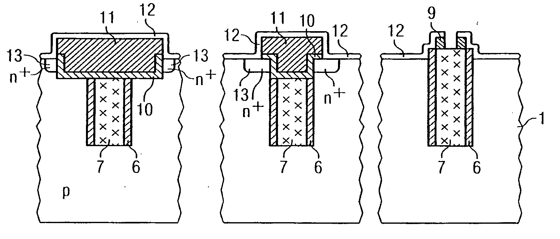
[0044]FIG. 2 shows a simplified sectional view of a semiconductor component with trench isolation in accordance with a second exemplary embodiment, identical reference symbols designating elements or layers identical or corresponding to those in FIG. 1, for which reason a repeated description is dispensed with below.

[0045]In accordance with FIG. 2, however, the semiconductor component may not only be formed in a semiconductor substrate with a multiple well structure, but rather may have merely a single doping, as a result of which, in particular for greatly simplified semiconductor circuits, improved shielding properties are likewise obtained with a reduced area requirement. The semiconductor component illustrated in FIG. 2 is an NMOS transistor, for example, a p-type semiconductor substrate 1 being used and, consequently, a p+-doped semiconductor material being used as electrically conductive filling layer. An improved connection possibility for the trench isolations that are conta...

third exemplary embodiment

[0047]FIG. 3 shows a simplified sectional view of a semiconductor component with trench isolation in accordance with a third exemplary embodiment, identical reference symbols designating elements or layers identical to those in FIG. 1 or 2 and a repeated description being dispensed with below.

[0048]In accordance with FIG. 3, the semiconductor substrate now has only a p-type well or an actual substrate 1 and an additional n-type well 2, the electrically conductive filling layer 7 being connected to the p-type well or the substrate 1. This yields an STI and TTI trench isolation for PMOS transistors, for which reason the doping regions 13 are p+-doped. Particularly when using highly doped semiconductor material, the electrically conductive filling layer is accordingly composed of a p′-doped polysilicon.

[0049]Improved shielding properties with a reduced area requirement again result in accordance with the first and secondary exemplary embodiment.


PUM


Abstract

The invention relates to a semiconductor component with trench isolation and to an associated fabrication method, a trench isolation (STI, TTI) having a deep isolation trench with a covering insulation layer (10, 11), a side wall insulation layer (6) and an electrically conductive filling layer (7), which is electrically connected to a predetermined doping region (1) of the semiconductor substrate in a bottom region of the trench. The use of a trench contact (DTC), which has a deep contact trench with a side wall insulation layer (6) and an electrically conductive filling layer (7), which is likewise electrically connected to the predetermined doping region (1) of the semiconductor substrate in a bottom region of the contact trench, makes it possible to improve the electrical shielding properties with a reduced area requirement.

Description

RELATED APPLICATIONS[0001]This application is a divisional application of U.S. patent application Ser. No. 10 / 523,239, filed Sep. 28, 2005, which is a national stage entry under 35 U.S.C 371 of PCT / DE03 / 02435, filed Jul. 19, 2003, which claims the benefit of priority to German Patent Application No. DE 10233208.8, filed Jul. 22, 2002.BACKGROUND[0002]1. Field of Application[0003]The present invention relates to a semiconductor component with trench isolation and to an associated fabrication method, and, in particular, to a semiconductor component with a trench-type, bottom-contact-connected active shielding and to an associated fabrication method.[0004]2. Background Information[0005]Isolations for defining, in particular, active regions in semiconductor substrates have usually been formed by thick oxide films, so-called local oxidation regions (LOCOS, Local Oxidation of Silicon). As the integration density rises, however, such conventional LOCOS methods are no longer suitable since t...

Claims


Application Information

Patent Timeline
IPC IPC(8): H01L21/762H01L21/76H01L21/28H01L21/763H01L27/08
CPCH01L21/76229H01L21/763H01L21/76232
Inventor SCHULER, FRANZTEMPEL, GEORG
Owner INFINEON TECH AG
Why Eureka
Try Eureka