Variable resistance non-volatile memory device and method for manufacturing the same

a non-volatile memory and variable resistance technology, which is applied in the direction of bulk negative resistance effect devices, coatings, chemical vapor deposition coatings, etc., can solve the problems of difficult temperature control of phase change materials, lowering the storage capacity of charge storage transistor type non-volatile memory, and reducing the resistance value in the off state. , the effect of lowering the resistance ratio

Inactive Publication Date: 2011-01-13
NEC CORP
View PDF2 Cites 33 Cited by
  • Summary
  • Abstract
  • Description
  • Claims
  • Application Information

AI Technical Summary

Benefits of technology

[0029]These defects may be the cause of formation of leakage current paths. That is, if there are many defects in a film, and a device is operated in a number of times, new defects are produced in the variable resistance material due to the leakage current. The value of the leakage current increases further and the resistance value in the OFF state keeps on to be reduced. As a result, the lowering of the ratio of the resistance in the ON state and that in the OFF state and t...

Problems solved by technology

However, if the insulating film which is for holding the electric charge, is reduced in thickness, the charge holding capability is lowered due to the increased leakage current.
It is thus becoming difficult to increase the storage capacity of the charge storage transistor type non-volatile memory.
Thus, if the device is used as a memory device or a switch, such a problem is met that the temperature control of the phase change material is difficult.
(1) The first problem is that, since the MIM variable resistance device is a two-terminal device, the current flowing at the time of the set/reset operations is difficult to control.
Hence, a large current may flow suddenly, thus possibly destructing the circuit.
Also, in the reset operation, a large current flows inevitably, when the device transferring to the OFF state.
In this case, there is a possibility that the large current ...

Method used


Image

  • Variable resistance non-volatile memory device and method for manufacturing the same
  • Variable resistance non-volatile memory device and method for manufacturing the same
  • Variable resistance non-volatile memory device and method for manufacturing the same

Examples


Embodiment Construction

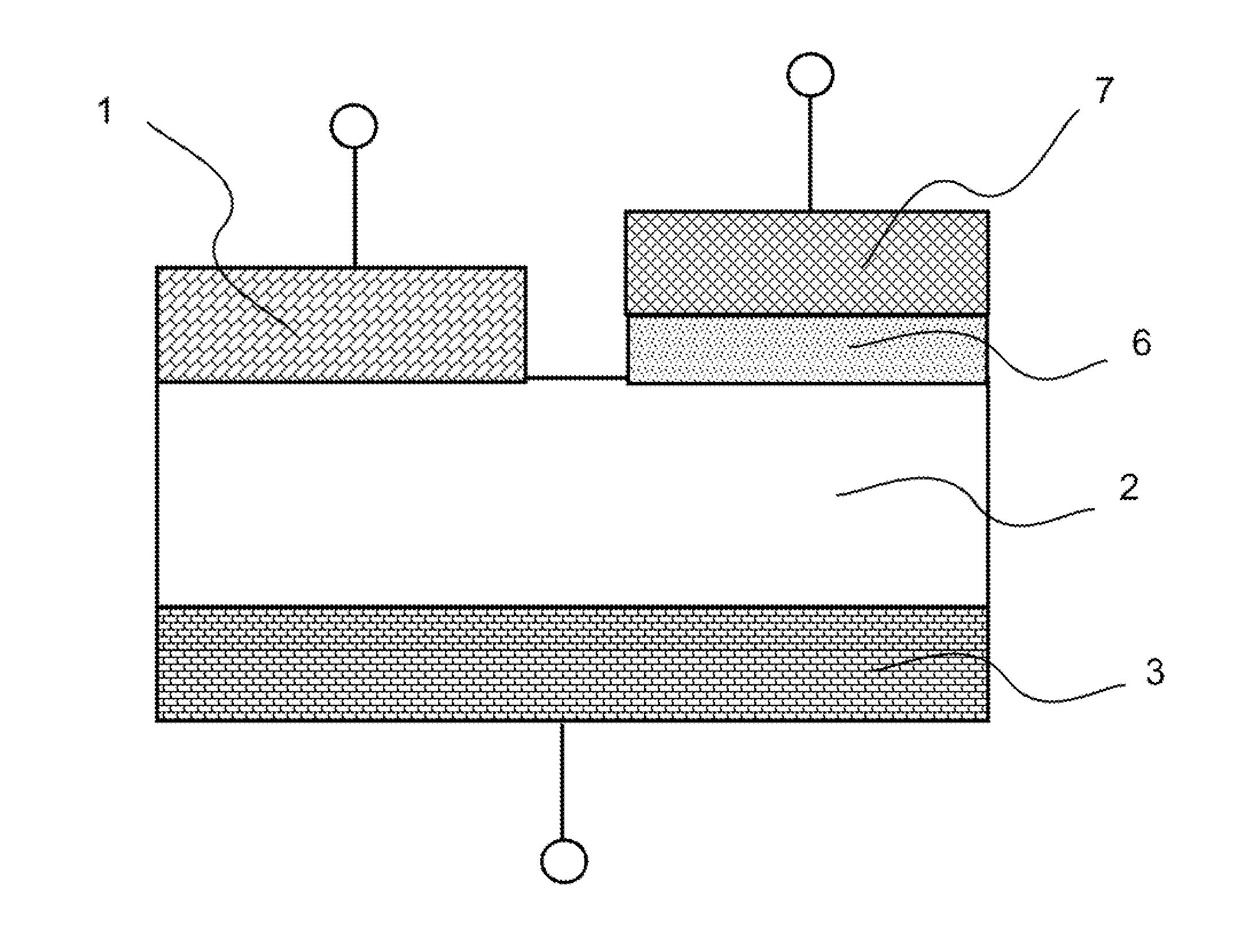
[0093]Exemplary embodiments of the present exemplary embodiment will now be described. In accordance with one of preferred modes of the present invention, there is provided a variable resistance non-volatile memory device (MIM type device) having a metal / variable resistance material / metal structure in which a variable resistance material (2) is sandwiched between metal electrodes (1, 3). An insulating film (6) is provided for being contacted with the variable resistance material (2). A voltage is applied to a reset electrode (7) which adapted for being contacted with the insulating film (6) without being contacted with the upper electrode (1) or with the lower electrode (3). By so doing, the MIM type device may be reset as scarcely any current is caused to flow. In addition, the current needed for the reset operation may be decreased without deteriorating the on / off resistance ratio in the switching operation of the MIM type device.

[0094]In one of preferred modes of the present inve...


PUM

PropertyMeasurementUnit
Densityaaaaaaaaaa
Electrical resistanceaaaaaaaaaa
Ratioaaaaaaaaaa

Abstract

A variable resistance non-volatile memory device of the laminated structure of an upper electrode a variable resistance material a lower electrode includes an insulating film formed for being contacted with the variable resistance material and a reset electrode formed for being contacted with the insulating film without being contacted with the upper electrode or the lower electrode. The device is reset by applying a voltage to the reset electrode. A low resistance value for the set state and a high resistance value for the reset state may be obtained as the current during the reset operation of the device is reduced. A low reset current and a high resistance ratio between the resistance value for the set state and that for the reset state are simultaneously achieved.

Description

REFERENCE TO RELATED APPLICATION [0001]This application is the National Phase of PCT / JP2009 / 051204, filed Jan. 26, 2009, which is based upon and claims the benefit of the priority of Japanese patent application No. 2008-016240 filed on Jan. 28, 2008, the disclosure of which is incorporated herein in its entirety by reference thereto.TECHNICAL FIELD[0002]This invention relates to a non-volatile MIM (metal-insulator-metal) memory device, and to a method for manufacture thereof.BACKGROUND ART[0003]The non-volatile memory, which has become a mainstream device in the marketplace, is implemented using a technique of varying a threshold value voltage of a semiconductor transistor by an electric charge accumulated within the bulk of an insulating film arranged above a channel region. Representative examples of such non-volatile memory include a flash memory and a SONOS (silicon-oxide-nitride-oxide-silicon) memory. To achieve a large storage capacity, the miniaturization of a transistor is i...

Claims


Application Information

Patent Timeline
IPC IPC(8): H01L45/00H01L21/16
CPCC23C16/406H01L27/101H01L27/24H01L45/08H01L45/085H01L45/1625H01L45/1226H01L45/1233H01L45/1253H01L45/146H01L45/1616H01L45/1206H10N70/24H10N70/245H10N70/253H10N70/826H10N70/8833H10N70/023
Inventor TAKAHASHI, KENSUKE
Owner NEC CORP
Why Eureka
Try Eureka