Method for manufacturing semiconductor device

a semiconductor layer and manufacturing method technology, applied in the field of methods, can solve problems such as oxidizing the oxide semiconductor layer, and achieve the effects of stable electric characteristics, improved electric characteristics, and high reliability

Active Publication Date: 2011-01-13
SEMICON ENERGY LAB CO LTD
View PDF99 Cites 34 Cited by
  • Summary
  • Abstract
  • Description
  • Claims
  • Application Information

AI Technical Summary

Benefits of technology

[0040]In accordance with the present invention, a thin film transistor having stable electric characteristics can be manufactured. In accordance with the present invention, a semiconductor device including a highly reliable thin film transistor having better electric characteristics can be manufactured.

Problems solved by technology

Further, the heat treatment can oxidize the oxide semiconductor layer.

Method used


Image

  • Method for manufacturing semiconductor device
  • Method for manufacturing semiconductor device
  • Method for manufacturing semiconductor device

Examples


embodiment 1

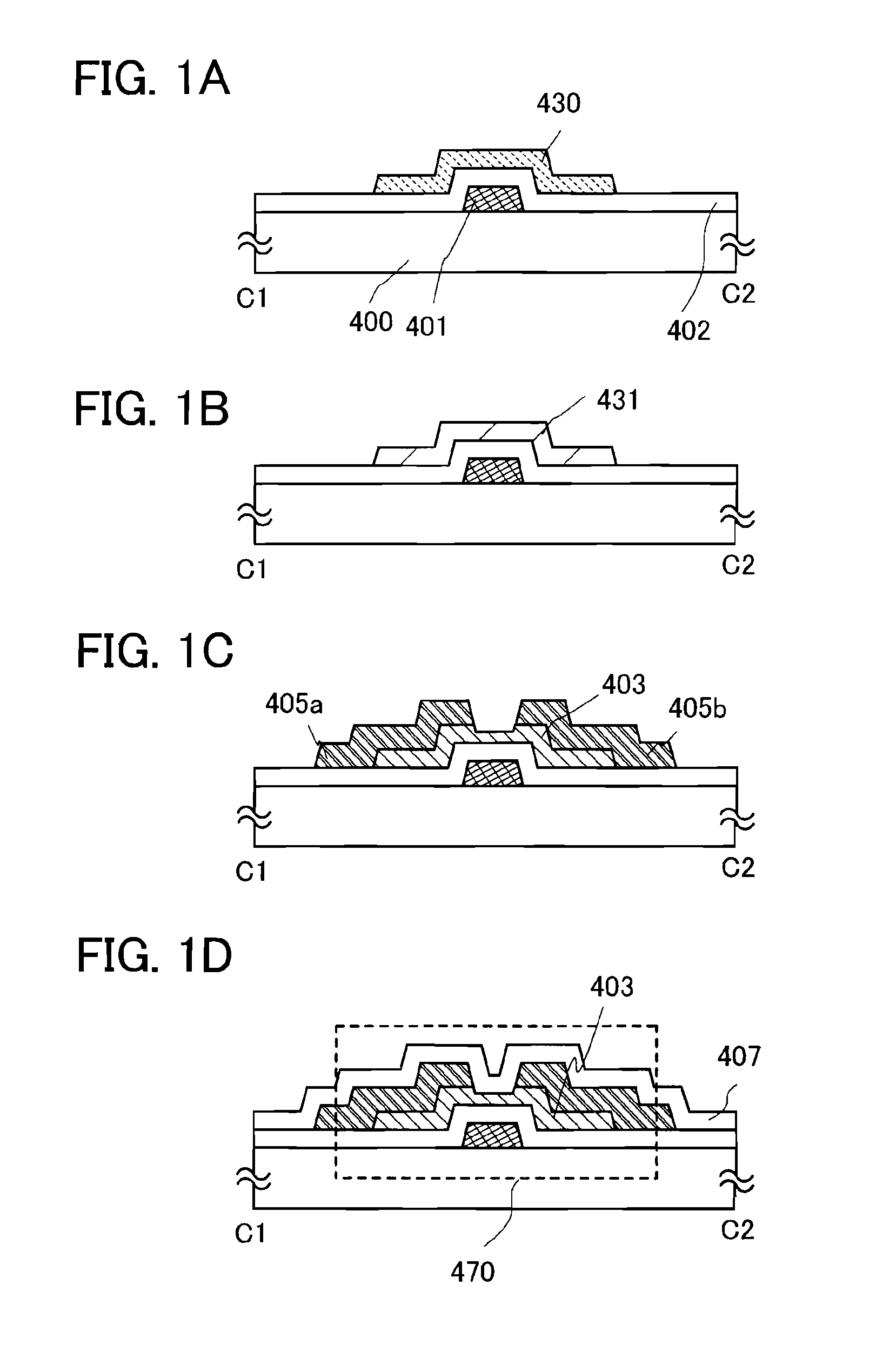
[0076]A semiconductor device and a method for manufacturing the semiconductor device will be described with reference to FIGS. 1A to 1D and FIGS. 2A and 2B.

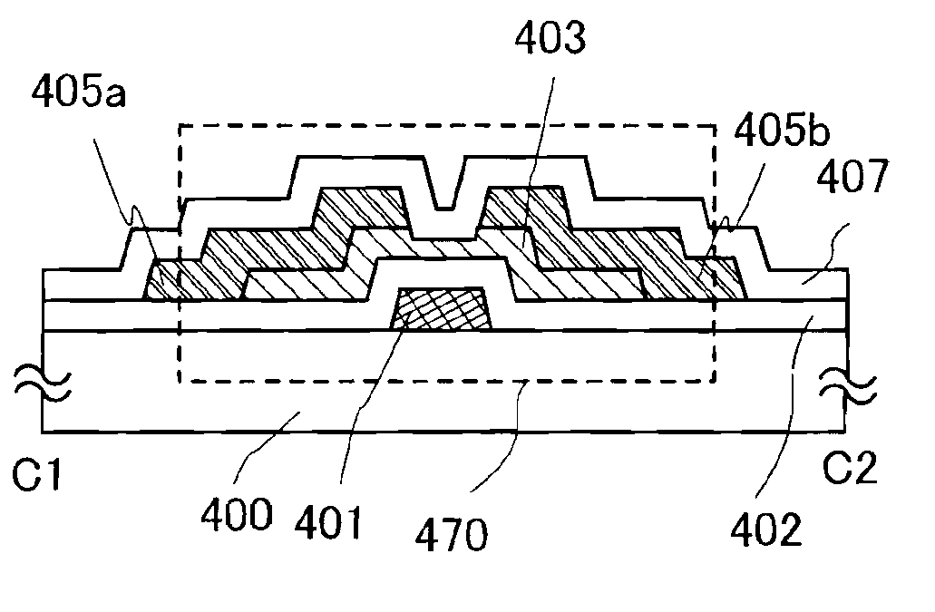
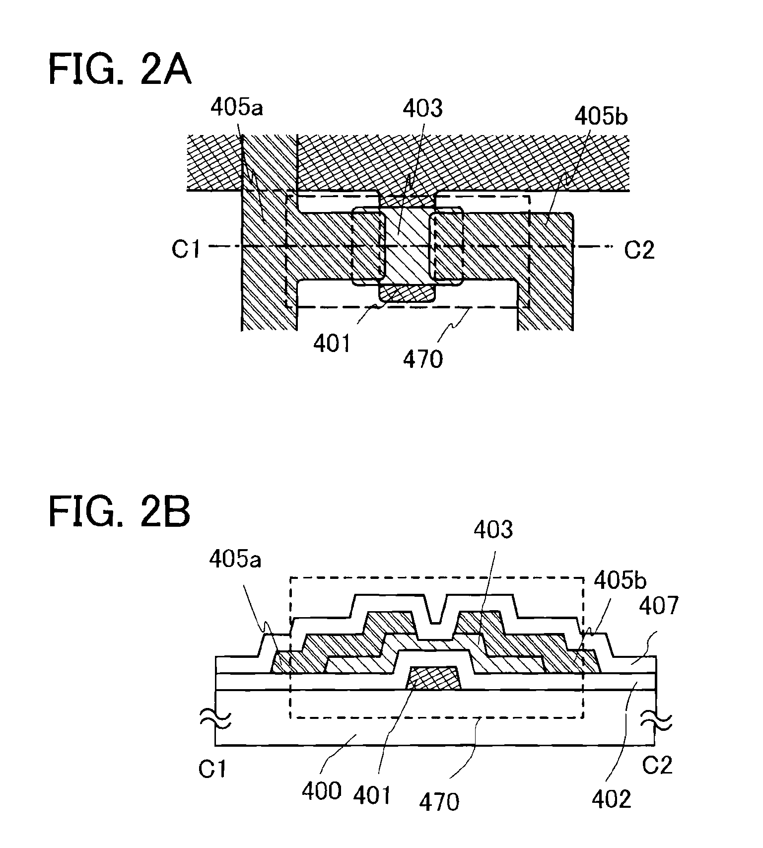
[0077]FIG. 2A is a plan view of a thin film transistor 470 included in a semiconductor device, and FIG. 2B is a cross-sectional diagram along line C1-C2 of FIG. 2A. The thin film transistor 470 is a bottom-gate thin film transistor and includes, over a substrate 400 which is a substrate having an insulating surface, a gate electrode layer 401, a gate insulating layer 402, an oxide semiconductor layer 403, and a source and drain electrode layers 405a and 405b. In addition, an oxide insulating layer 407 is provided to cover the thin film transistor 470 and be in contact with the oxide semiconductor layer 403.

[0078]As for the oxide semiconductor layer 403, heat treatment which reduces impurities such as moisture (heat treatment for dehydration or dehydrogenation) is performed in an oxygen atmosphere at least after the formation of t...

embodiment 2

[0123]A semiconductor device and a method for manufacturing the semiconductor device will be described with reference to FIGS. 4A to 4D and FIGS. 5A and 5B. Embodiment 1 can be applied to the same portion(s), or a portion(s) or a step(s) having the similar function(s) as / to Embodiment 1, and the description thereof is not repeated.

[0124]FIG. 5A is a plan view of a thin film transistor 460 included in a semiconductor device, and FIG. 5B is a cross-sectional diagram along line D1-D2 of FIG. 5A. The thin film transistor 460 is a bottom-gate thin film transistor and includes, over a substrate 450 which is a substrate having an insulating surface, a gate electrode layer 451, a gate insulating layer 452, a source and drain electrode layers 455a and 455b, and an oxide semiconductor layer 453. In addition, an oxide insulating layer 457 is provided to cover the thin film transistor 460 and be in contact with the oxide semiconductor layer 453.

[0125]In the thin film transistor 460, the gate in...

embodiment 3

[0145]A process for manufacturing a semiconductor device including a thin film transistor will be described with reference to FIGS. 6A to 6D, FIGS. 7A to 7C, 8, and 9A1, 9A2, 9B1, and 9B2.

[0146]In FIG. 6A, as a substrate 100 having light-transmitting property, the substrate 100 described in Embodiment 1 can be used as appropriate.

[0147]Next, a conductive layer is formed entirely over a surface of the substrate 100, and then a first photolithography process is performed to form a resist mask. Then, an unnecessary portion is removed by etching, so that wirings and electrodes (a gate wiring including a gate electrode layer 101, a capacitor wiring 108, and a first terminal 121) are formed. At this time, the etching is performed so that at least end portions of the gate electrode layer 101 are tapered.

[0148]The gate wiring including the gate electrode layer 101, the capacitor wiring 108, and the first terminal 121 in a terminal portion each can be formed using a material of the gate elec...


PUM


Abstract

A highly reliable semiconductor device which includes a thin film transistor having stable electric characteristics, and a manufacturing method thereof. In the manufacturing method of the semiconductor device which includes a thin film transistor where a semiconductor layer including a channel formation region is an oxide semiconductor layer, heat treatment which reduces impurities such as moisture to improve the purity of the oxide semiconductor layer and oxidize the oxide semiconductor layer (heat treatment for dehydration or dehydrogenation) is performed. Not only impurities such as moisture in the oxide semiconductor layer but also those existing in a gate insulating layer are reduced, and impurities such as moisture existing in interfaces between the oxide semiconductor layer and films provided over and under and in contact with the oxide semiconductor layer are reduced.

Description

TECHNICAL FIELD[0001]The present invention relates to a semiconductor device including an oxide semiconductor and a manufacturing method thereof.[0002]In this specification, a semiconductor device generally refers to any device which can function by utilizing semiconductor characteristics: an electro-optic device, a semiconductor circuit, and an electronic device are all included in the category of the semiconductor device.BACKGROUND ART[0003]In recent years, a technique by which a thin film transistor (TFT) is manufactured using a semiconductor thin layer (having a thickness of about several nanometers to several hundred nanometers) formed over a substrate having an insulating surface has attracted attention. Thin film transistors have been applied to a wide range of electronic devices such as ICs or electro-optic devices and urgently developed particularly as switching elements in image display devices. Various metal oxides are used for a variety of applications. Indium oxide is a...

Claims


Application Information

Patent Timeline
Patent Type & Authority Applications(United States)
IPC IPC(8): H01L21/36H05B44/00
CPCH01L27/1225H01L29/66969H01L21/477H01L29/7869H01L29/78696G02F1/1362
Inventor YAMAZAKI, SHUNPEIHOSOBA, MIYUKINODA, KOSEIOHARA, HIROKISASAKI, TOSHINARISAKATA, JUNICHIRO
Owner SEMICON ENERGY LAB CO LTD
Why Eureka
Try Eureka