Semiconductor device

Active Publication Date: 2011-01-20
PANASONIC CORP
View PDF9 Cites 21 Cited by
  • Summary
  • Abstract
  • Description
  • Claims
  • Application Information

AI Technical Summary

Benefits of technology

[0029]According to the semiconductor devices of the present invention, an electron supply layer (fourth semiconductor layer) which is undoped or doped with an n-type impurity is left in a region excluding the gate electrode formation portion thereof. Therefore, the distance between the upper surface of the nitride semiconductor and

Problems solved by technology

Therefore, even when a positive gate voltage is applied,

Method used


Image

  • Semiconductor device
  • Semiconductor device
  • Semiconductor device

Examples


Example

First Embodiment

[0081]A first embodiment of the present invention will be described with reference to the accompanying drawings.

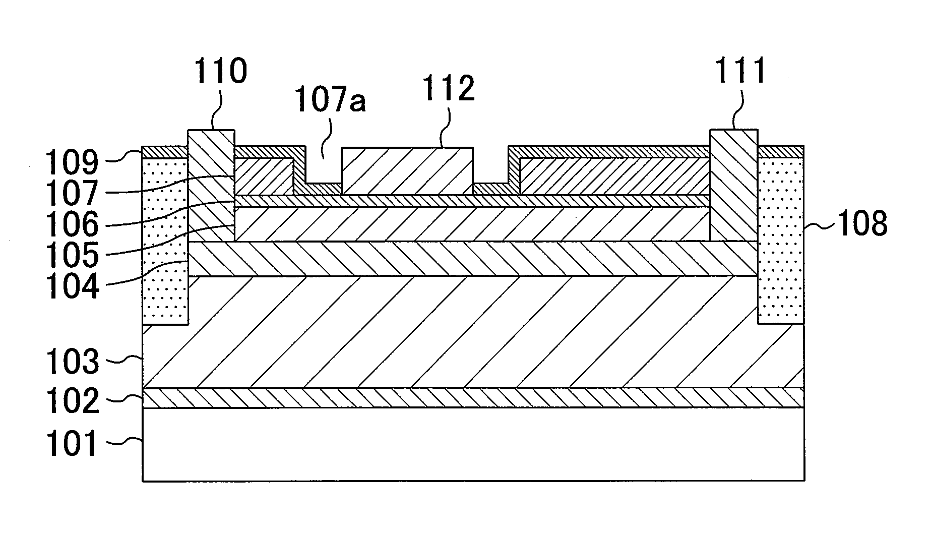
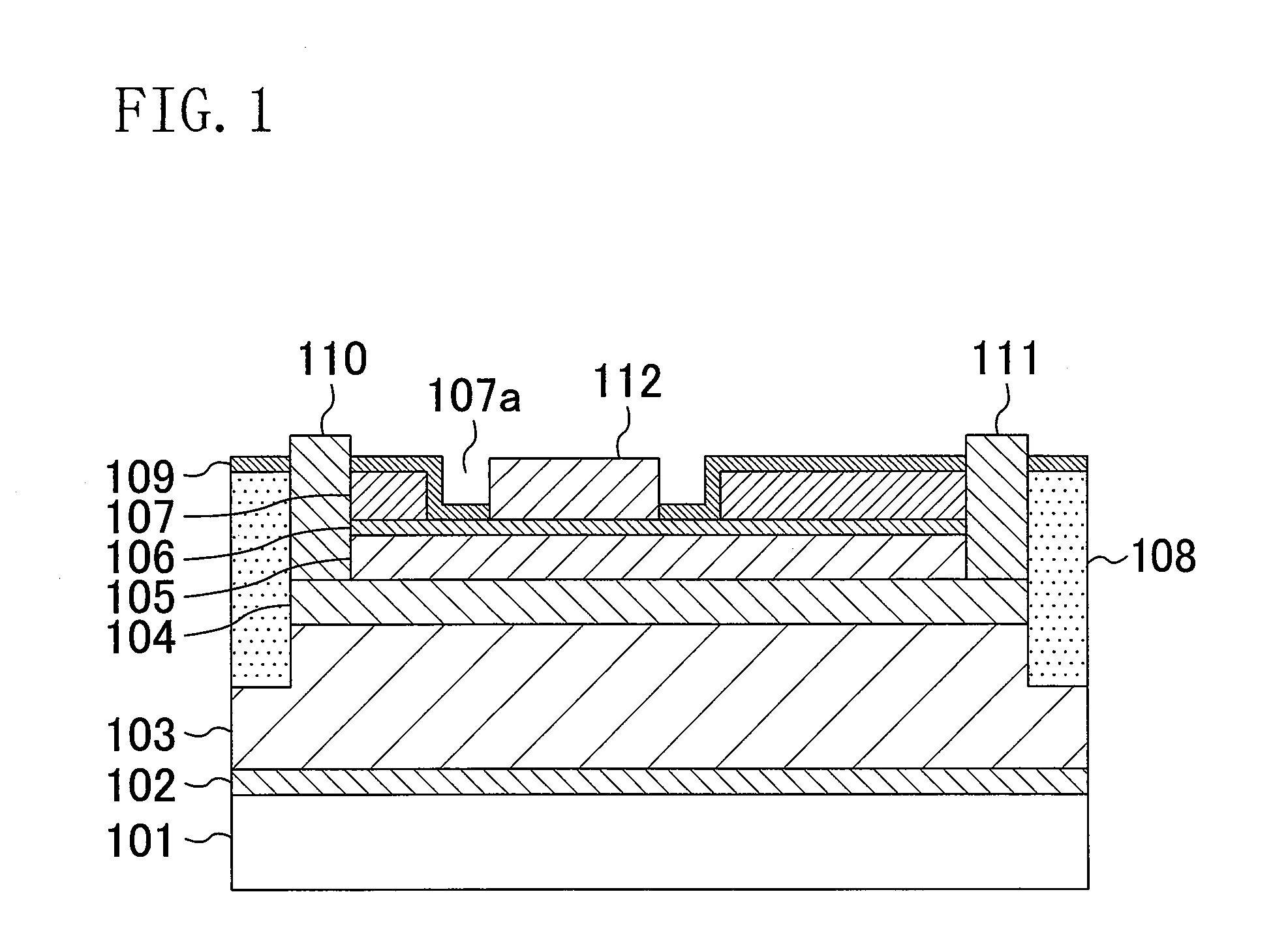
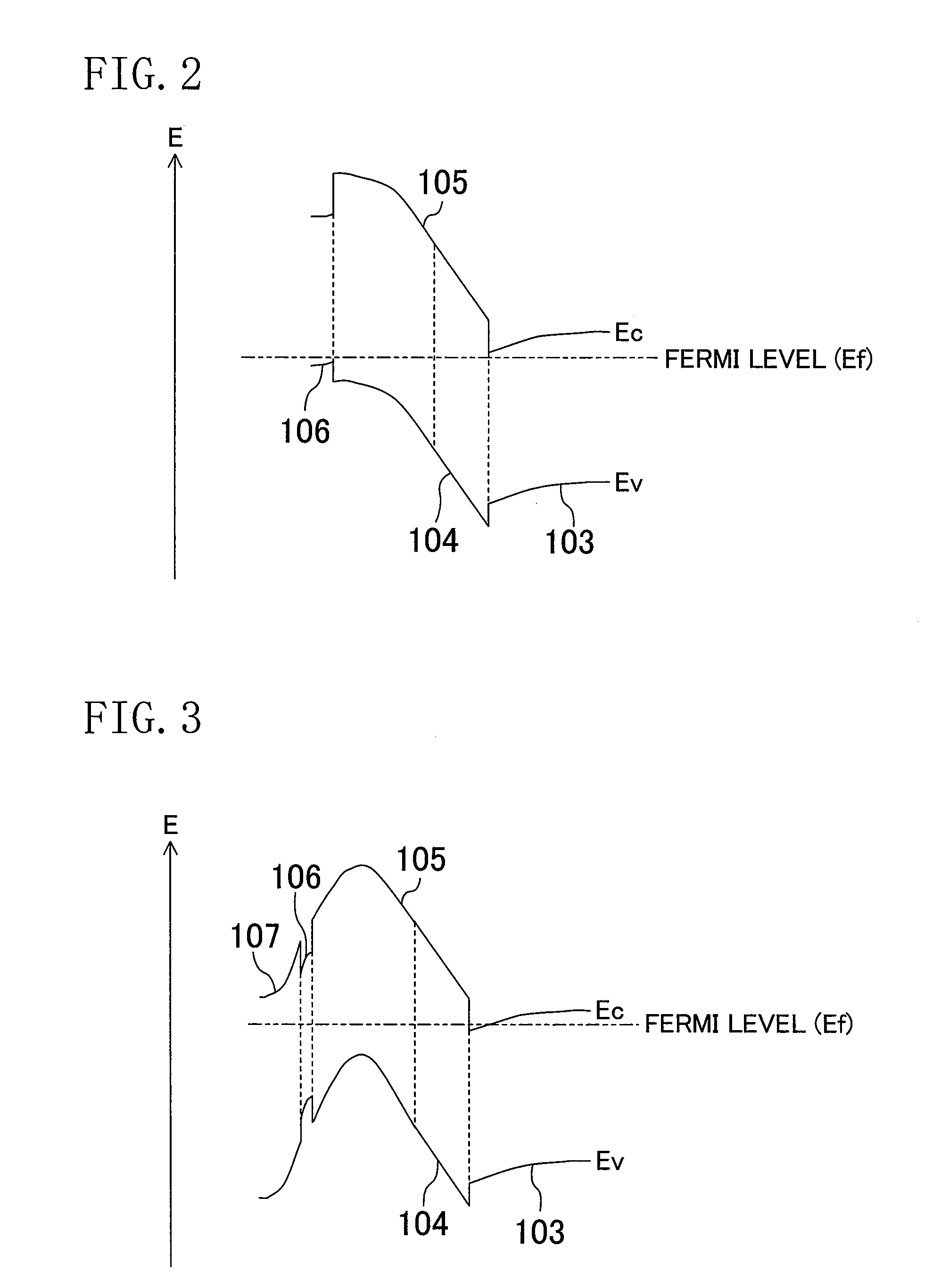
[0082]FIG. 1 is a cross-sectional view of a configuration of a field effect transistor which is a semiconductor device according to a first embodiment of the present invention. As shown in FIG. 1, the field effect transistor of the first embodiment includes a buffer layer 102 made of aluminum nitride (AlN) having a thickness of 100 nm, an undoped gallium nitride (GaN) layer 103 having a thickness of 2 μm, an undoped aluminum gallium nitride (AlGaN) layer 104 having a thickness of 25 nm, a p-type AlGaN layer 105 having a thickness of 50 nm, a high-concentration p-type GaN layer 106 having a thickness of 5 nm, and an n-type AlGaN layer 107 having a thickness of 20 nm, which are successively formed, by epitaxial growth, on a main surface of a substrate 101 made of sapphire, where the main surface has a plane orientation (0001) (i.e., a (0001) plane). Here, the...

Example

Second Embodiment

[0092]A second embodiment of the present invention will be described hereinafter with reference to the drawings.

[0093]FIG. 5 is a cross-sectional view of a configuration of a field effect transistor which is a semiconductor device according to a second embodiment of the present invention. As shown in FIG. 5, the field effect transistor of the second embodiment includes a buffer layer 202 made of aluminum nitride (AlN) having a thickness of 100 nm, an undoped gallium nitride (GaN) layer 203 having a thickness of 2 μm, an undoped aluminum gallium nitride (AlGaN) layer 204 having a thickness of 25 nm, a p-type composition gradient AlGaN layer 205 having a thickness of 50 nm, a high-concentration p-type GaN layer 206 having a thickness of 5 nm, an n-type composition gradient AlGaN layer 207 having a thickness of 20 nm, which are successively formed, by epitaxial growth, on a main surface of a substrate 201 made of sapphire, where the main surface has a plane orientation...

Example

Third Embodiment

[0104]A third embodiment of the present invention will be described hereinafter with reference to the drawings.

[0105]FIG. 8 is a cross-sectional view of a configuration of a field effect transistor which is a semiconductor device according to a third embodiment of the present invention. As shown in FIG. 8, the field effect transistor of the third embodiment includes a buffer layer 302 made of AlN having a thickness of 100 nm, an undoped GaN layer 303 having a thickness of 2 μm, an undoped AlGaN layer 304 having a thickness of 25 nm, an undoped indium gallium (InGaN) layer 305 having a thickness of 5 nm, and an undoped AlGaN layer 306 having a thickness of 20 nm, which are successively formed, by epitaxial growth, on a main surface of a substrate 301 made of sapphire, where the main surface has a plane orientation (0001) (i.e., a (0001) plane). Here, the Al composition of each of the AlGaN layers 304 and 306 is assumed to be 25%, and the In composition of the undoped ...


PUM


Abstract

A semiconductor device includes an undoped GaN layer (103) formed on a substrate (101), an undoped AlGaN layer (104) formed on the undoped GaN layer (103) and having a band gap energy larger than that of the undoped GaN layer (103), a p-type AlGaN layer (105) and a high-concentration p-type GaN layer (106) formed on the undoped AlGaN layer (104), and an n-type AlGaN layer (107) formed on the high-concentration p-type GaN layer (106). A gate electrode (112) which makes ohmic contact with the high-concentration p-type GaN layer (106) is formed on the high-concentration p-type GaN layer (106) in a region thereof exposed through an opening (107a) formed in the n-type AlGaN layer (107).

Description

TECHNICAL FIELD[0001]The present invention relates to semiconductor devices made of a nitride semiconductor which are applicable to power transistors for use in, for example, power supply circuits for consumer apparatuses and the like.BACKGROUND ART[0002]Group III nitride semiconductors, such as notably gallium nitride (GaN), are wide gap semiconductors. For example, gallium nitride (GaN) and aluminum nitride (AlN) have energy gaps of as large as 3.4 eV and 6.2 eV, respectively, at room temperature. The Group III nitride semiconductors also have large breakdown electric fields, and higher electron saturation velocities than those of compound semiconductors such as gallium arsenide (GaAs) and the like, silicon (Si), and the like. Due to these properties, field effect transistors (FETs) made of a GaN-based compound semiconductor material, which are used as high frequency electronic devices or high power electronic devices, have been vigorously studied and developed.[0003]Nitride semic...

Claims


Application Information

Patent Timeline
IPC IPC(8): H01L29/12
CPCH01L29/2003H01L29/41766H01L29/7786H01L29/432H01L29/66462H01L29/4236
Inventor UMEDA, HIDEKAZUHIKITA, MASAHIROUEDA, TETSUZOTANAKA, TSUYOSHIUEDA, DAISUKE
Owner PANASONIC CORP
Why Eureka
Try Eureka