Image capture device

Active Publication Date: 2011-02-17
SAMSUNG ELECTRONICS CO LTD
View PDF10 Cites 31 Cited by
  • Summary
  • Abstract
  • Description
  • Claims
  • Application Information

AI Technical Summary

Benefits of technology

[0032]Since the image capture device of the present invention uses a dispersive element, first of all, high sensitivity is achieved without causing any optical loss. In addition, since a light ray with green (G) component, which will achieve high luminous efficacy, is incident on a photosensitive cell that faces the dispersive

Problems solved by technology

On top of that, in a normal color camera, a subtractive organic dye filter (color filter) that uses an organic pigment as a dye is arranged over each photosensing section of an image sensor, and therefore, the optical efficiency achieved is rather low.
It is true that the

Method used


Image

  • Image capture device
  • Image capture device
  • Image capture device

Examples


Example

Embodiment 1

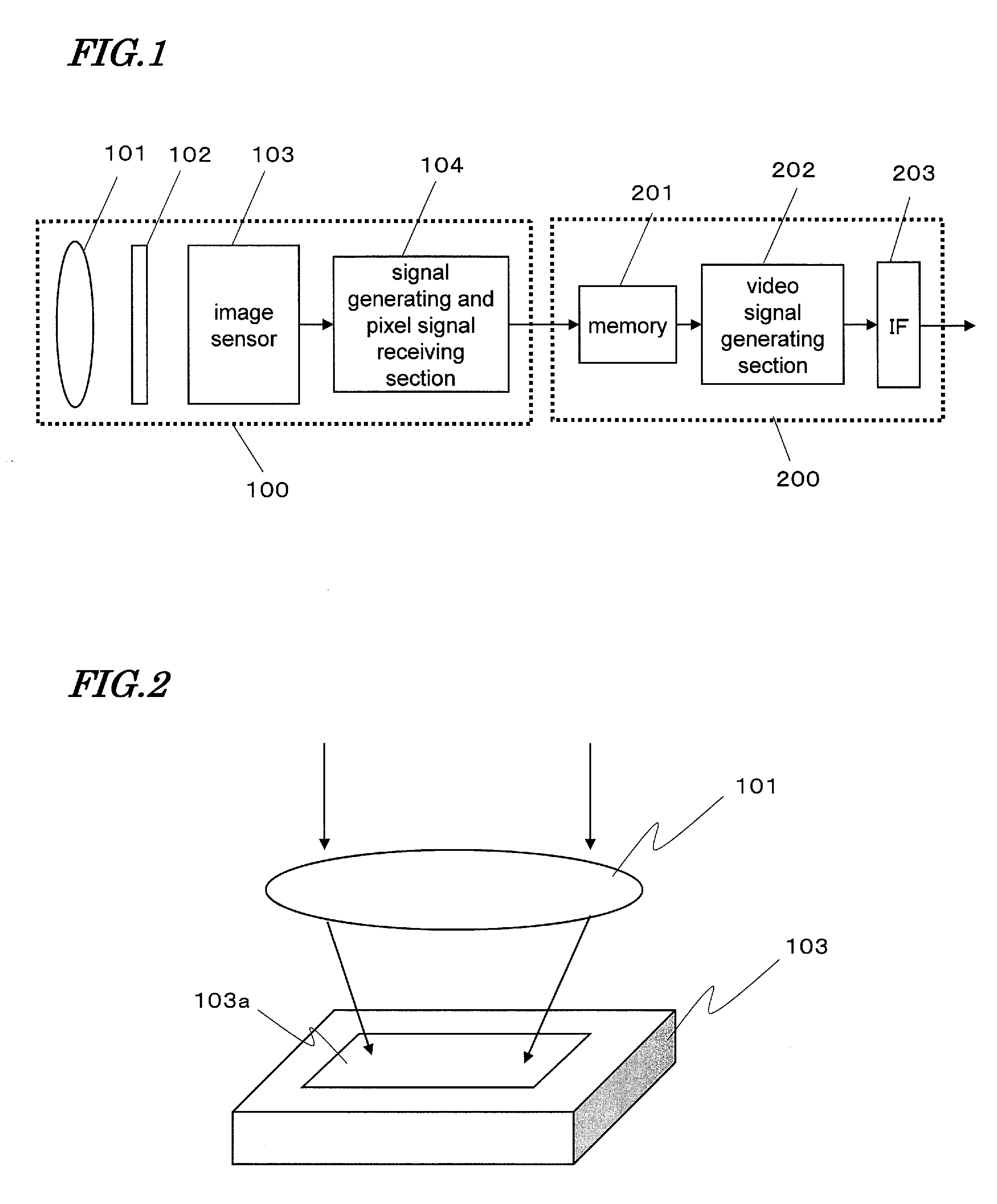
[0045]FIG. 1 is a block diagram illustrating an overall configuration for an image capture device as a first specific preferred embodiment of the present invention. The Image capture device shown in FIG. 1 includes an image capturing section 100 and a signal processing section 200 that receives a signal from the image capturing section 100 and generates a video signal. The configuration and operation of the image capturing section 100 and the signal processing section 200 will be described.

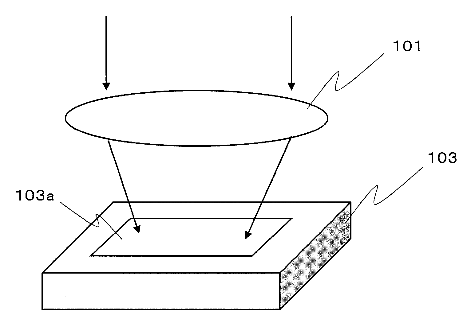
[0046]The image capturing section 100 includes a lens 101 for imaging a given subject, an optical plate 102, an image sensor 103 for converting optical information, which has been collected by imaging the subject through the lens 101 and the optical plate 102, into an electrical signal by photoelectric conversion, and a signal generating and pixel signal receiving section 104. In this case, the optical plate 102 is a combination of a quartz crystal low-pass filter for reducing a moiré ...

Example

Embodiment 2

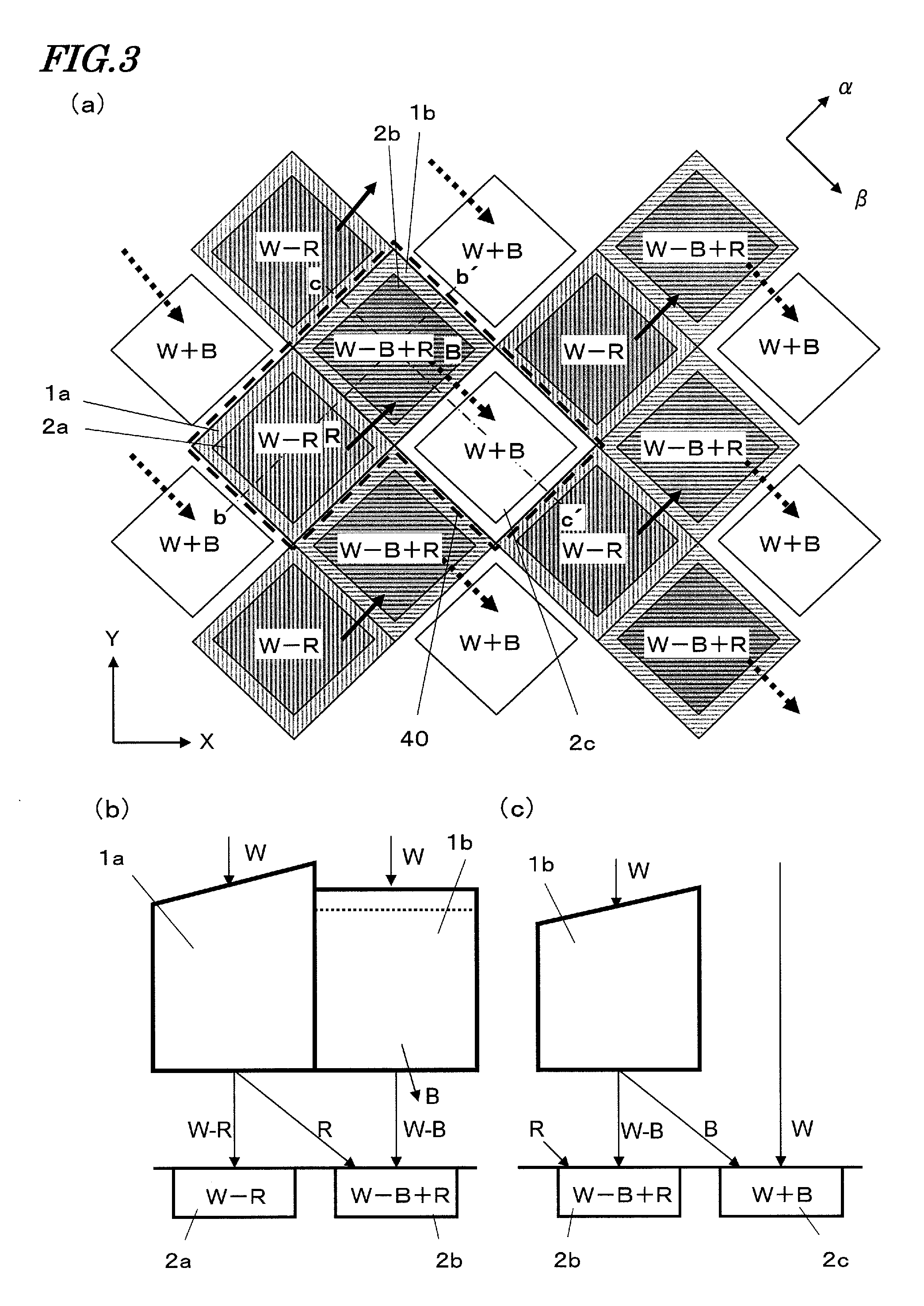
[0068]Hereinafter, a second specific preferred embodiment of the present invention will be described with reference to FIGS. 4(a) to 4(c) and FIG. 5. The image capture device of this preferred embodiment has quite the same configuration as the counterpart of the first preferred embodiment described above except its solid-state image sensor. Thus, the following description will be focused on only the differences from the first preferred embodiment described above. In the following description, any component having substantially the same function as its counterpart of the first preferred embodiment described above will be identified by the same reference numeral as the one used for the first preferred embodiment.

[0069]FIG. 4(a) is a pixel plan view illustrating a part of an array of dispersive elements, a part of an array of photosensitive cells and how light is split in a solid-state image sensor according to this preferred embodiment. On the other hand, FIGS. 4(b) and 4(...

Example

Embodiment 3

[0082]Hereinafter, a third specific preferred embodiment of the present invention will be described with reference to FIGS. 6(a) to 6(c). The image capture device of this preferred embodiment has quite the same configuration as the counterpart of the first preferred embodiment described above except its solid-state image sensor. Thus, the following description will be focused on only the differences from the first preferred embodiment described above. In the following description, any component having substantially the same function as its counterpart of the first preferred embodiment described above will be identified by the same reference numeral as the one used for the first preferred embodiment.

[0083]FIG. 6(a) is a pixel plan view illustrating a part of an array of dispersive elements, a part of an array of photosensitive cells and how light is split in a solid-state image sensor according to this preferred embodiment. On the other hand, FIGS. 6(b) and 6(c) are cross...


PUM


Abstract

A color representation technique to be effectively applicable to a pixel shifted arrangement to realize high sensitivity and high resolution is provided by using a dipersive prism or diffraction.
A dispersive element is provided for an image sensor in which photosensitive cells are arranged to be shifted from each other by a half pitch both horizontally and vertically. The dispersive element makes at least G rays fall straight down to a pixel right under itself and also makes either R rays or B rays incident on an adjacent pixel. Meanwhile, a photosensitive cell, for which no dispersive element is provided, receives directly incident light, too. Color information can be obtained by making computations on photoelectrically converted signals provided by these pixels.

Description

TECHNICAL FIELD[0001]The present invention relates to a solid-state imaging device structure for use in an image capture device.BACKGROUND ART[0002]Recently, the performance and functionality of digital cameras and digital movie cameras that use some solid-state imaging device such as a CCD and a CMOS (which will be sometimes referred to herein as an “image sensor”) have been enhanced to an astonishing degree. In particular, the size of a pixel structure for use in a solid-state imaging device has been further reduced these days thanks to development of semiconductor device processing technologies, thus getting an even greater number of pixels and drivers integrated together in a solid-state imaging device. As a result, the resolution of an image sensor has lately increased significantly from one million pixels to ten million pixels in a matter of few years. Meanwhile, the greater the number of pixels in an image sensor, the lower the intensity of the light falling on a single pixel...

Claims


Application Information

Patent Timeline
IPC IPC(8): H04N5/228H04N5/335
CPCG02B5/045G02B27/42H04N9/045H01L27/14625H01L27/14603H04N23/84
Inventor HIRAMOTO, MASAOYONEMOTO, KAZUYASUGITANI, YOSHIAKI
Owner SAMSUNG ELECTRONICS CO LTD
Why Eureka
Try Eureka