Method and apparatus for measuring wafer bias potential

a technology of bias potential and measuring apparatus, which is applied in the direction of resistance/reactance/impedence, electric discharge tubes, instruments, etc., can solve the problems of affecting the effectiveness of the wafer processing system, and affecting the accuracy of the measurement. achieve the effect of reducing the number of measurements, reducing the cost of measurement, and prolonging the lifetim

Active Publication Date: 2011-02-24
LAM RES CORP
View PDF20 Cites 54 Cited by
  • Summary
  • Abstract
  • Description
  • Claims
  • Application Information

AI Technical Summary

Benefits of technology

[0027]Unfortunately, conventional methods for measuring the wafer potential are inaccurate, have short lifetimes, are prone to errors and require significant effort for maintenance and configuration. What is needed is a method for measuring the wafer potential that is accurate, has a prolonged lifetime, is not prone to errors and does not require a significant amount of effort for maintenance and configuration.
[0028]It is an object of the present invention to provide an apparatus for measuring the wafer potential located in a plasma processing system that is accurate, provides a sustained lifetime, is not prone to errors and provides for ease of maintenance and configuration.

Problems solved by technology

The DC bias potential increases the energy of the ion presented to the wafer and consequently alters the effectiveness of the wafer processing system.
Excessively large bias voltages in the range of 400V to 500V can damage the oxide film on the surface of a wafer.
Direct measurement of wafer potential is very difficult.
It is virtually impossible to attach or connect a probe to the wafer for direct measurement of the wafer potential, as probes are incapable of withstanding the harsh environment surrounding the wafer.
While these conventional methods are capable of providing an estimate of the wafer potential, each method has issues with respect to accuracy, longevity, maintenance, configuration and / or potential for errors.
This method for processing wafers can be difficult to calibrate and configure as a result of the complex load transition errors which occur in the estimated potential of wafer 102.
Unfortunately, the use of these electrodes produces contaminants within the process chamber, as the electrodes are erroded by the plasma.
This contamination negatively impacts the effectiveness of the plasma by reducing the plasma etch rate.
Additionally, the electrodes are consumable and must frequently be replaced requiring significant time, effort and cost.
These contaminates negatively impact the effectiveness of the plasma by reducing the plasma etch rate.
Additionally, the electrodes are consumable and must frequently be replaced requiring significant time, effort and cost.
Hence, the ESC leakage current detection method for estimating the wafer potential requires considerable time, effort and cost for calibration and configuration.
Unfortunately, conventional methods for measuring the wafer potential are inaccurate, have short lifetimes, are prone to errors and require significant effort for maintenance and configuration.

Method used


Image

  • Method and apparatus for measuring wafer bias potential
  • Method and apparatus for measuring wafer bias potential
  • Method and apparatus for measuring wafer bias potential

Examples


Embodiment Construction

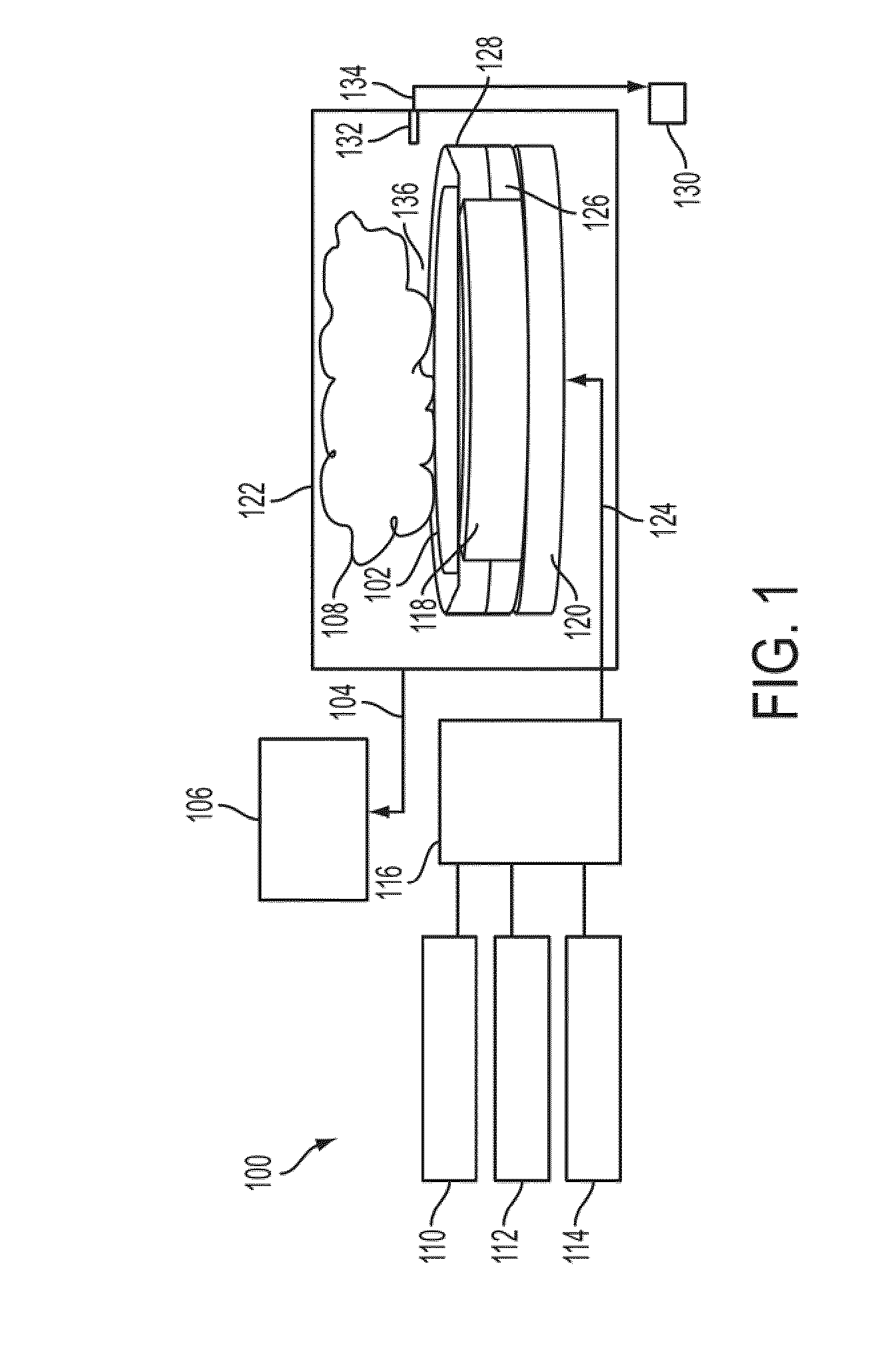
[0042]In accordance with an aspect of the present invention, an HER is used as a plasma sheath voltage transducer to monitor wafer potential in a wafer processing system. Accordingly, in accordance with an aspect of the present invention, voltage probe is not exposed to the plasma as with conventional systems discussed above with reference to FIGS. 1 and 2.

[0043]Aspects of the present inventions will now be described with reference to FIGS. 3-10B.

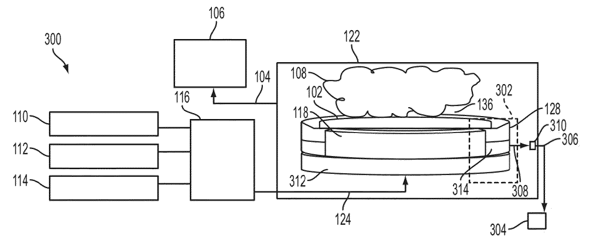
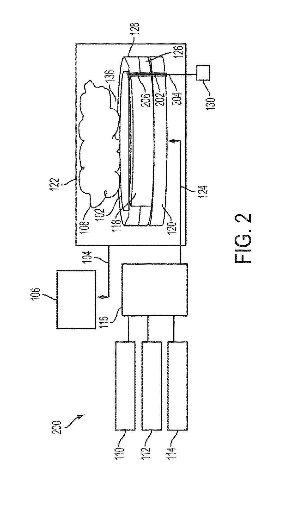
[0044]FIG. 3 illustrates an example of a wafer processing system 300 in accordance with an aspect of the present invention. Wafer processing system 300 contains several common elements wafer processing system 200 of FIG. 2. However, wafer processing system 300 does not include probe 202 and electrical conductor 204. Wafer processing system 300 further includes a signal conditioner 310 and a processor 304. Additionally, ESC base plate 120 and ceramic coupling ring 126 of wafer processing system 200 have been replaced with an ESC base plate 3...


PUM


Abstract

A device for use in a wafer processing chamber having a plasma forming volume and a hot edge ring. The hot edge ring has a first surface and a second surface. The first surface is in contact with the plasma forming volume. The second surface is not in contact with the plasma forming volume. The device includes a detector operable to contact the second surface of the hot edge ring. The detector can detect a parameter of the hot edge ring and can provide a detected signal based on the detected parameter.

Description

BACKGROUND[0001]The present invention relates to wafer processing chambers. More particularly, the present invention relates to an apparatus for measuring the DC bias potential of a wafer during plasma processing.[0002]In conventional wafer processing systems, it is common to affix the wafer to the lower electrode pedestal with an electrostatic attraction force provided by an electrostatic chuck (ESC). Electrostatic chucking is commonly implemented by providing a conductive film between two insulation films located on the upper surface of the pedestal. Once a semiconductor wafer is affixed to the ESC, the wafer may be processed.[0003]In the conventional production of semiconductor integrated circuits, plasma is used to promote ionization of a process gas for etching, chemical vapor deposition or sputtering a wafer. In a conventional capacitive plasma processing system, upper and lower electrodes, e.g., large area parallel plates, are provided in a pressure-controlled process chamber...

Claims


Application Information

Patent Timeline
Patent Type & Authority Applications(United States)
IPC IPC(8): G01R27/08
CPCH01J37/32935H01J37/32642
Inventor MAKHRATCHEV, KONSTANTINVALCORE, JOHN
Owner LAM RES CORP
Why Eureka
Try Eureka