Fault detection in electroluminescent displays

Inactive Publication Date: 2011-02-24
GLOBAL OLED TECH
View PDF20 Cites 37 Cited by
  • Summary
  • Abstract
  • Description
  • Claims
  • Application Information

AI Technical Summary

Benefits of technology

[0017]The present invention has the advantage that, by providing a display device with embedded chiplet control and fault detection, improved performance, improved routing, and manufacturing yields are improved. A serial shift register for communication provides a simple and flexible way to control the display device.

Problems solved by technology

However, the efficiency of organic materials in particular, decreases as the organic materials are used.
However, a passive-matrix drive device is limited in the number of rows (or columns) that can be included in the device since the sequential nature of the row (or column) driving creates flicker.
If too many rows are included, the flicker can become perceptible.
Moreover, the currents necessary to drive an entire row (or column) in a display can be problematic since the power required for the non-imaging pre-charge and discharge steps of PM driving become dominant as the area of the PM display grows.
These problems limit the physical size of a passive-matrix display.
Thin-film transistors (TFTs) made from amorphous or polycrystalline silicon are relatively large and have lower performance compared to conventional transistors made in crystalline silicon wafers.
Moreover, such thin-film devices typically exhibit local or large-area non-uniformity across the glass substrate that results in non-uniformity in the electrical performance and visual appearance of displays employing such materials.
The wiring and circuitry requirements of this design, however, can further reduce the substrate area available for light emission.
Since a conventional passive-matrix display design is limited in size and number of light-emitting elements, an active-matrix design using TFTs has lower electrical performance and complex substrates as well as significant wiring requirements, and device testing and fault detection is important for manufacturing yield and display lifetime,

Method used


Image

  • Fault detection in electroluminescent displays
  • Fault detection in electroluminescent displays
  • Fault detection in electroluminescent displays

Examples


Embodiment Construction

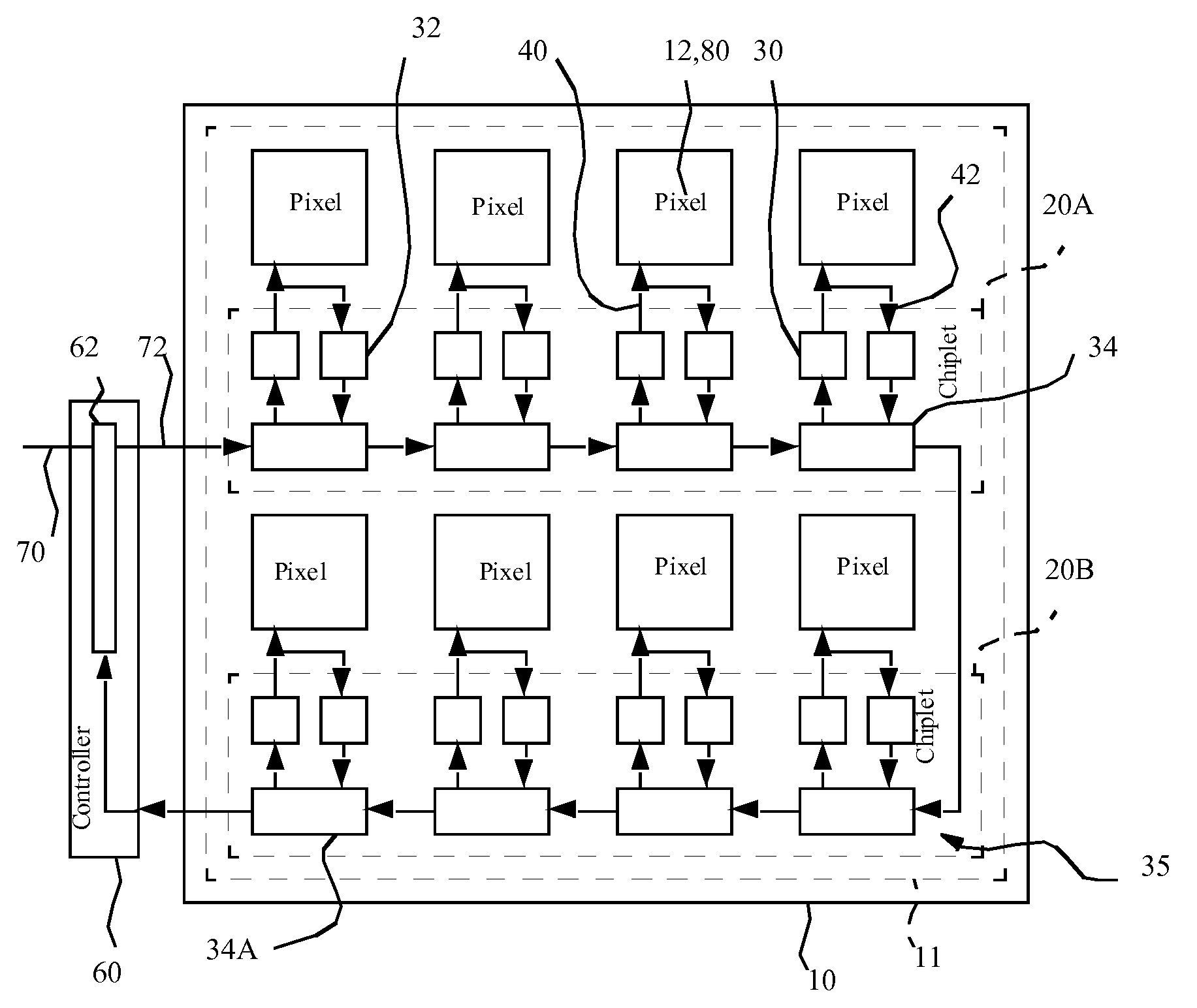
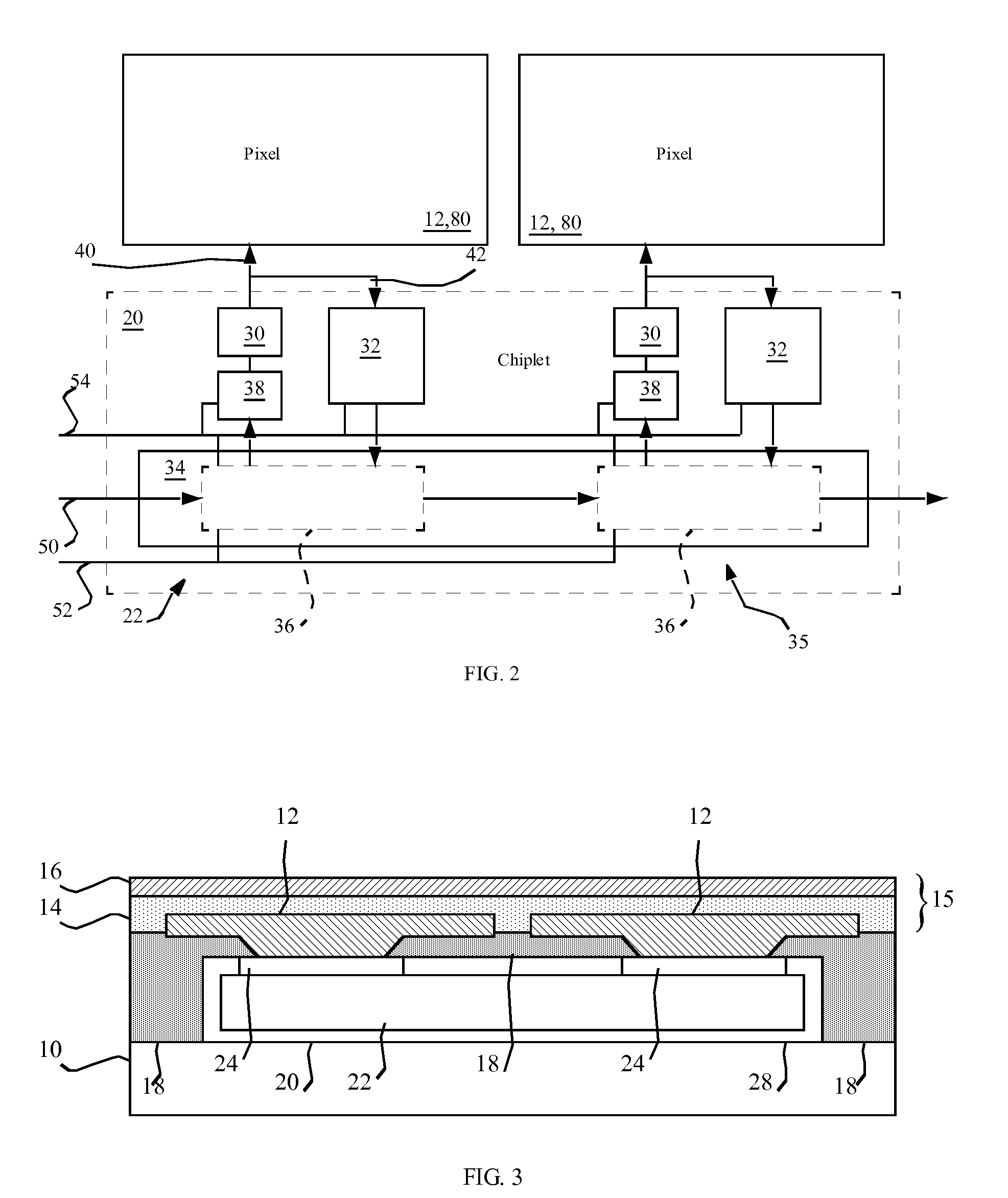
[0026]Referring to FIGS. 1 and 3, in one embodiment of the present invention, a display device includes a display substrate 10 having a display area 11. A plurality of pixels 80 are formed over the display substrate 10 in the display area 11, each pixel including a first electrode 12, one or more layers of light-emitting material 14 formed over the first electrode 12, and a second electrode 16 formed over the one or more layers of light-emitting material 14, the light-emitting material emitting light 14 in response to a current passed through the light-emitting material 14 by the first and the second electrodes 12, 16 with a driven electrical signal. A driving circuit 30 is located in the display area 11 for each driven electrical signal, the driving circuit 30 providing the driven electrical signal 40 corresponding to a desired pixel luminance value 72 to the first or second electrode 12, 16 of the pixel 80, the driven electrical signal 40 producing a current passed through the lig...


PUM


Abstract

Detecting faults in driving circuits within a display device is disclosed. The display device has an array of pixels formed over a substrate in a display area, each pixel having a driving circuit and an associated communication circuit, the communication circuits together forming a multi-pixel serial shift register. The multi-pixel serial shift register is used to shift desired pixel luminance values from a display controller through the multi-pixel serial shift register to corresponding driving circuits for driving the pixels with driven electrical signals to emit light corresponding to the desired pixel luminance values, and sensing electrical signals corresponding to the driven electrical signals with a sensing circuit. Further the sensed electrical signals are shifted by the multi-pixel serial shift register to the display controller and faults are detected in the driving circuits by analyzing the sensed electrical signals.

Description

FIELD OF THE INVENTION[0001]The present invention relates to fault detection in display devices having a substrate with distributed, independent chiplets for controlling a pixel array and for communicating with the pixel array.BACKGROUND OF THE INVENTION[0002]Flat-panel display devices are widely used in conjunction with computing devices, in portable devices, and for entertainment devices such as televisions. Such displays typically employ a plurality of pixels distributed over a substrate to display images. Each pixel incorporates several, differently colored light-emitting elements commonly referred to as sub-pixels, typically emitting red, green, and blue light, to represent each image element. As used herein, pixels and sub-pixels are not distinguished and refer to a single light-emitting element. A variety of flat-panel display technologies are known, for example plasma displays, liquid crystal displays, and light-emitting diode (LED) displays.[0003]Light emitting diodes (LEDs...

Claims


Application Information

Patent Timeline
IPC IPC(8): G09G5/10G09G3/30H01J9/24
CPCG09G3/006G09G3/2085G09G2360/148G09G2320/0295G09G2320/04G09G3/3208G09G3/30H05B33/10
Inventor COK, RONALD S.
Owner GLOBAL OLED TECH
Why Eureka
Try Eureka