3D optoelectronic packaging

a technology of optoelectronic packaging and optical transceivers, applied in semiconductor lasers, semiconductor/solid-state device details, instruments, etc., can solve the problems of affecting the performance of the current optical transceiver

Active Publication Date: 2011-02-24
GLOBALFOUNDRIES US INC
View PDF3 Cites 75 Cited by
  • Summary
  • Abstract
  • Description
  • Claims
  • Application Information

AI Technical Summary

Problems solved by technology

Current use of electrical data links perform best over short distances, but they reach a performance limit as the link distance and frequency increases.
Optical data links over fiber are capable of high speed communication with low loss over large distances, however, current optical transceivers are bulky and expensive compared with their electrical counterparts.

Method used


Image

  • 3D optoelectronic packaging
  • 3D optoelectronic packaging
  • 3D optoelectronic packaging

Examples


Embodiment Construction

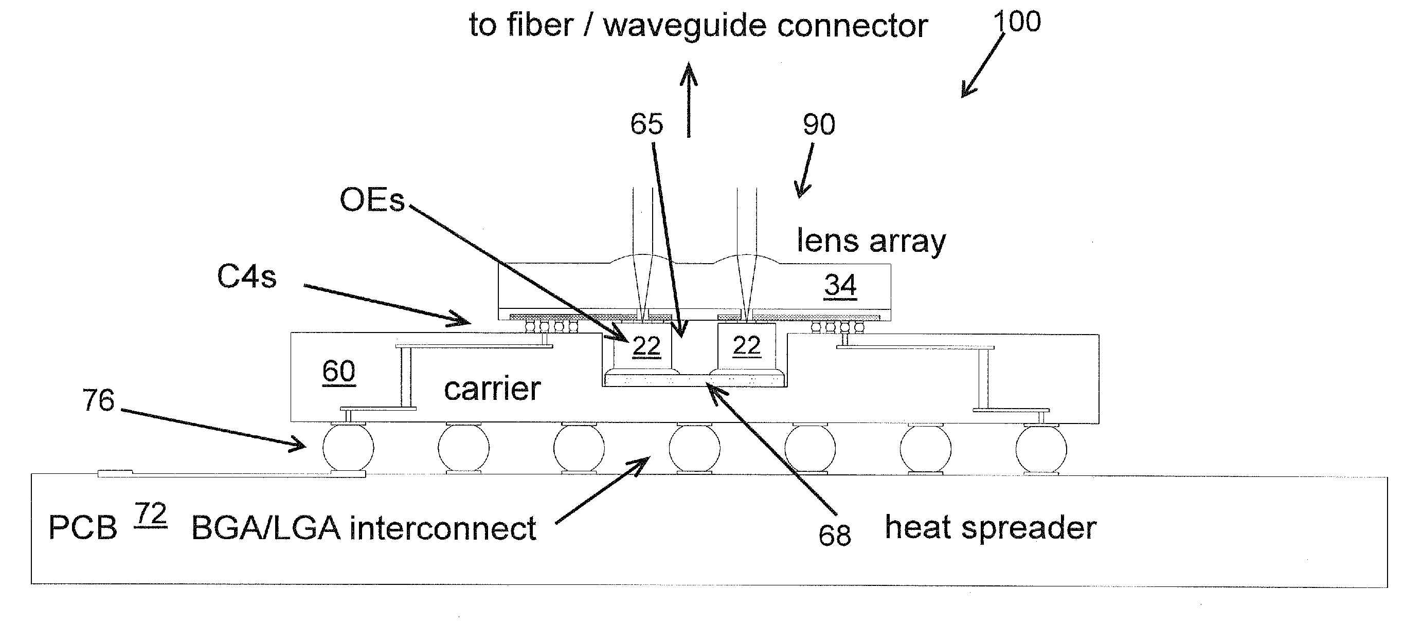
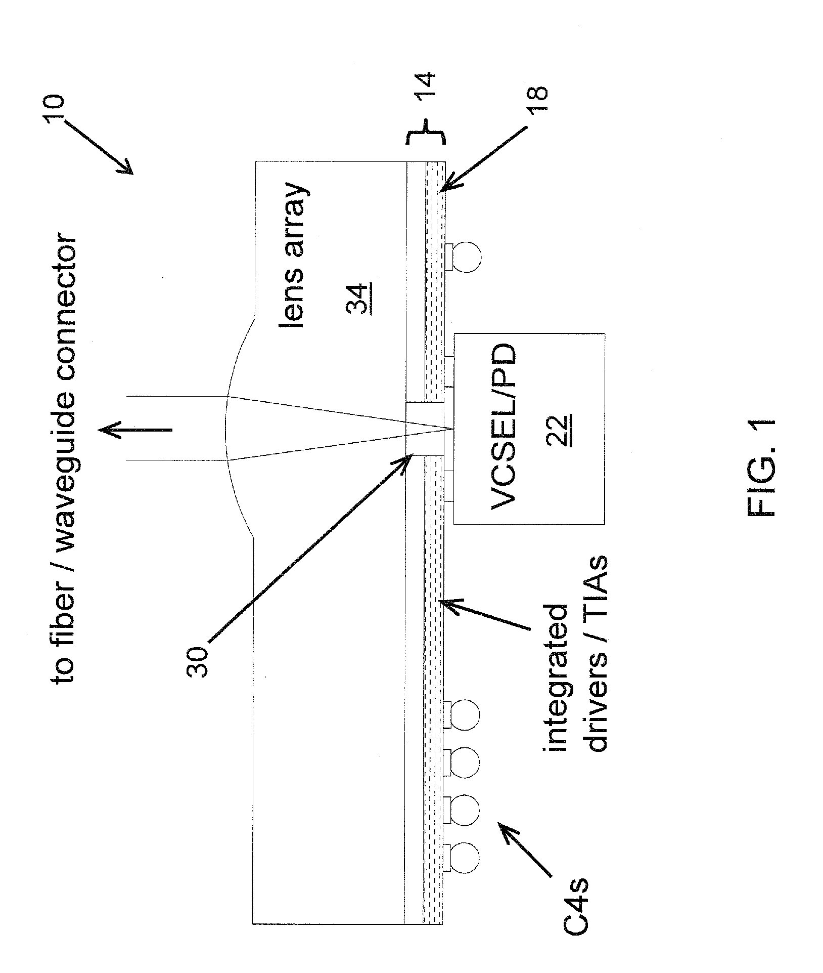
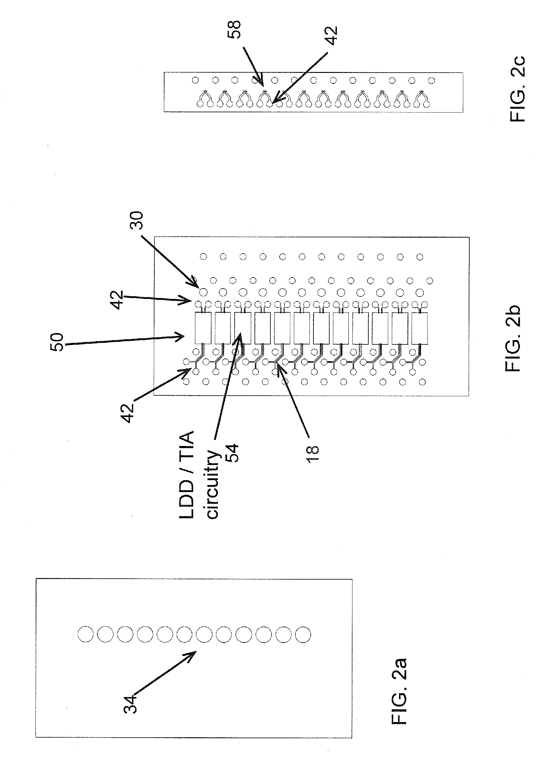
Referring to FIG. 1, an integrated OE assembly 10 includes a silicon wafer 14 (or thinned silicon) having circuitry / wiring layers 18. The circuitry / wiring layers 18 drive an OE element embodied as a laser diode array (e.g., vertical cavity surface emitting lasers (VCSEL)) and / or amplifies the signals from a photodiode (PD) array, collectively referred to as a VCSEL / PD or OE array 22. The OE arrays 22 communicate with laser diode drivers (LDD) and transimpedance amplifiers (TIAs) collectively referred to as LDD / TIA circuitry 50, shown in FIG. 2b. In the embodiment of the invention show in FIG. 1, LDD drivers and / or TIAs are integrated in the wiring circuitry, using LDD / TIA circuitry 54, shown in FIG. 2b.

It is understood that an OE element may be comprised of either active or passive components, and may serve an optical function (send, receive, direct or pass light) and an electrical function (process, amplify signals, wiring, or electrical pads, or contacts).

In one embodiment of the...


PUM


Abstract

An optoelectronic (OE) package or system and method for fabrication is disclosed which includes a silicon layer with a wiring layer. The silicon layer has an optical via for allowing light to pass therethrough. An optical coupling layer is bonded to the silicon layer, and the optical coupling layer includes a plurality of microlenses for focusing and or collimating the light through the optical via. One or more first OE elements are coupled to the silicon layer and electrically communicating with the wiring. At least one of the first OE elements positioned in optical alignment with the optical via for receiving the light. A second OE element embedded within the wiring layer. A carrier may be interposed between electrical interconnect elements and positioned between the wiring layer and a circuit board.

Description

BACKGROUNDThe present invention relates generally to the field of integrated circuits and silicon chip technology, and more particularly, relates to a packaging system or packaging assembly and method thereof for optoelectronic devices in integrated circuits and silicon chip technology.Computer system performance is increasingly important in current computer systems and data centers, including for example, personal computers, servers and server farms. Computer performance is measured by, for example, system availability, speed of computation, processor speed, among other measurable aspects. The communication bandwidth between computers and within a computer is important in a computer system's overall performance. The current trend towards multi-core processors and multiple processors per machine requires an increase in communication between processors, and between a processor and its memory. Current use of electrical data links perform best over short distances, but they reach a per...

Claims


Application Information

Patent Timeline
Patent Type & Authority Applications(United States)
IPC IPC(8): H01S5/026H01L31/0232H01L21/50
CPCG02B6/4201G02B6/4206H01L2924/10253H01L2924/3011H01L2924/15311G02B6/4249G02B6/4292H01L23/367H01L25/16H01L27/1446H01L27/14625H01L2224/131H01L2924/01046H01L2924/14H01L2924/1433H01L2924/15153H01L2924/15192H01L2924/014H01L2924/00G02B6/4245G02B6/4257G02B6/4266G02B6/4269G02B6/428
Inventor BUDD, RUSSELL A.FORTIER, PAULLIBSCH, FRANK R.
Owner GLOBALFOUNDRIES US INC
Why Eureka
Try Eureka