Method and system for MEMS devices

a technology of microelectricalmechanical devices and methods, applied in the direction of microstructural systems, acceleration measurement using interia forces, instruments, etc., can solve the problems of devices up to 80%) being relegated to the packaging area, special challenges in fabrication and packaging technologies, etc., to achieve accurate depositing and defining metals, shift in performance, inherent hermeticity and conductivity

Inactive Publication Date: 2011-03-03
MIRADIA INC
View PDF15 Cites 136 Cited by
  • Summary
  • Abstract
  • Description
  • Claims
  • Application Information

AI Technical Summary

Benefits of technology

Embodiments of the present invention provide a method for bonding substrates using eutectic bonding techniques in the fabrication of a MEMS package. Eutectic reactions are a triple point in the phase diagram where solid alloys mixtures transform directly to a liquid phase. Upon cooling, a microstructure is formed, which is both strong and hermetic. Eutectic metal compositions have several benefits as sealing materials, including the ability to accurately deposit and define the metals

Problems solved by technology

Since MEMS contain by definition some sort of mechanical function, they present special challenges to fabrication and packaging technologies.
While fabrication technologies have largely kept pace with market d

Method used


Image

  • Method and system for MEMS devices
  • Method and system for MEMS devices
  • Method and system for MEMS devices

Examples


Embodiment Construction

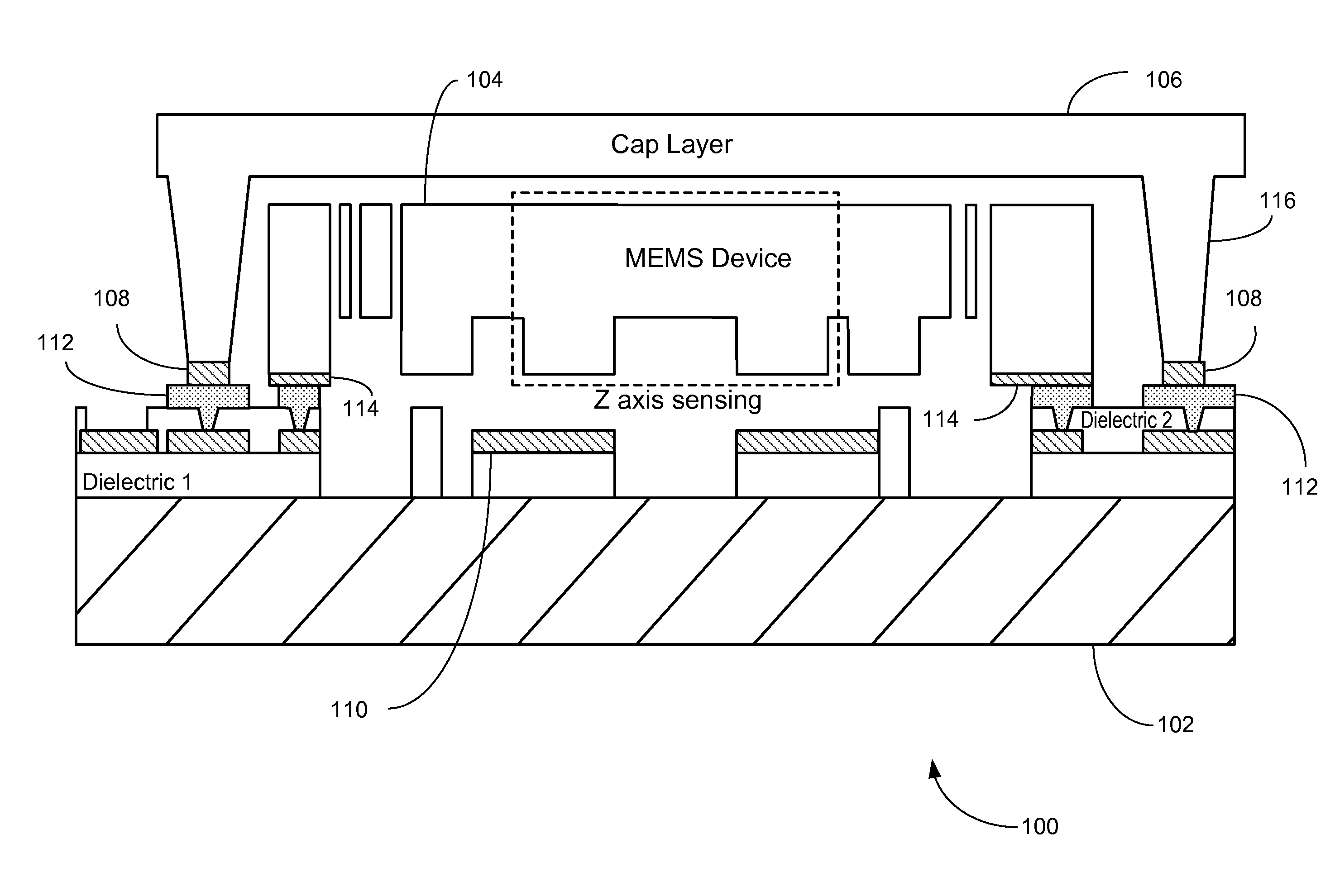
According to the embodiments of the present invention, semiconductor processing techniques are provided. More particularly, embodiments of the present invention include a method and structure for forming MEMS devices using semiconductor fabrication techniques. Merely by way of example, an embodiment provides a method of forming accelerometers and gyroscopes using a monolithic integration process, thereby reducing the die footprint by at least a factor of two. The method and structure can be applied to other applications as well, such as actuators, sensors, and detectors.

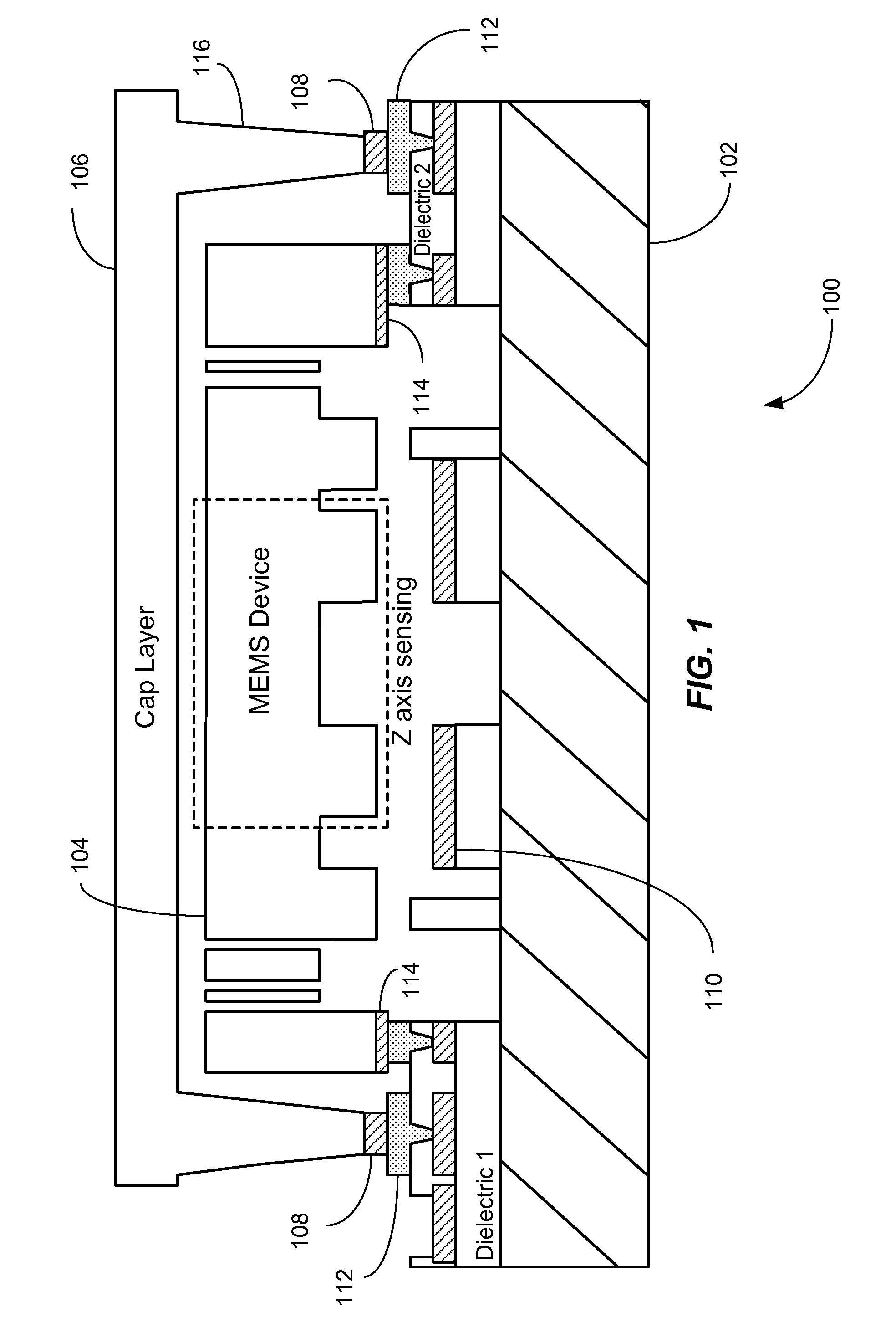
FIG. 1 illustrates a cross-sectional view of a MEMS device assembly 100 according to an embodiment of the present invention. MEMS device assembly 100 includes a base substrate 102. In some embodiments, base substrate 102 can be a silicon substrate. Base substrate 102 includes a plurality of electrodes 110 disposed on an upper surface. Base substrate 102 also includes a plurality of conductive bonding regions 112 that...


PUM


Abstract

A micro electro-mechanical (MEMS) device assembly is provided. The MEMS device assembly includes a first substrate that has a plurality of electronic devices, a plurality of first bonding regions, and a plurality of second bonding regions. The MEMS device assembly also includes a second substrate that is bonded to the first substrate at the plurality of first bonding regions. A third substrate having a recessed region and a plurality of standoff structures is disposed over the second substrate and bonded to the first substrate at the plurality of second bonding regions. The plurality of first bonding regions provide a conductive path between the first substrate and the second substrate and the plurality of the second bonding regions provide a conductive path between the first substrate and the third substrate.

Description

BACKGROUNDMicroelectrical-mechanical systems (MEMS) devices have experienced impressive and steady growth as they have integrated into people's everyday lives. Since their conceptualization in the 1970's, they have progressed from laboratory curiosity to integration in high-end systems, and, more recently, to widespread application in popular consumer devices.A number of factors have fueled the growth in demand for MEMS devices, ranging from gains in performance and functionality to new processes to lower the manufacturing cost for the devices, to fundamental changes in the technology and materials used in the device manufacturing. Since MEMS contain by definition some sort of mechanical function, they present special challenges to fabrication and packaging technologies. While fabrication technologies have largely kept pace with market demand, the enormous difficulties in packaging such devices have weighed down its progress, resulting in an inappropriate proportion of costs (for so...

Claims


Application Information

Patent Timeline
IPC IPC(8): H01L29/84H01L21/50
CPCB81B2201/0235B81B2207/015B81C2203/0735B81C1/00269B81C2203/0109B81C1/00246
Inventor WU, HUA-SHUCHIEN, YU-HAOCHUNG, SHIH-YUNGTSENG, LI-TIENYEH, YU-TE
Owner MIRADIA INC
Why Eureka
Try Eureka