Imaging device and camera system

a technology which is applied in the field of imaging device and camera system, can solve the problems of limited application of image sensor, high cost of transfer interface and chip for subsequent image processing, and significant difficulties in digitizing data, so as to improve imaging performance, eliminate analog signal processing, and reduce the number of apertures of pixels

Active Publication Date: 2011-03-03
SONY CORP
View PDF5 Cites 87 Cited by
  • Summary
  • Abstract
  • Description
  • Claims
  • Application Information

AI Technical Summary

Benefits of technology

[0067]The embodiments of the invention can eliminate handling of analog signals to cancel out circuit noise originated from an AD converter and handling analog signals, without reducing the number of apertures of pixels, thereby improving the imaging performance at a low cost.

Problems solved by technology

However, significant difficulties still remain in digitizing the data and making the best use of the imaged data stored in the memory 19.
First, when a vast amount of data acquired at the frame rate several ten times faster is transferred outside as it is, the transfer interface and the chip for the subsequent image processing become very expensive.
If the frame rate is merely increased considerably over the sensing ability of eyes, application of the image sensor is limited.

Method used


Image

  • Imaging device and camera system
  • Imaging device and camera system
  • Imaging device and camera system

Examples


first embodiment

2. First Embodiment

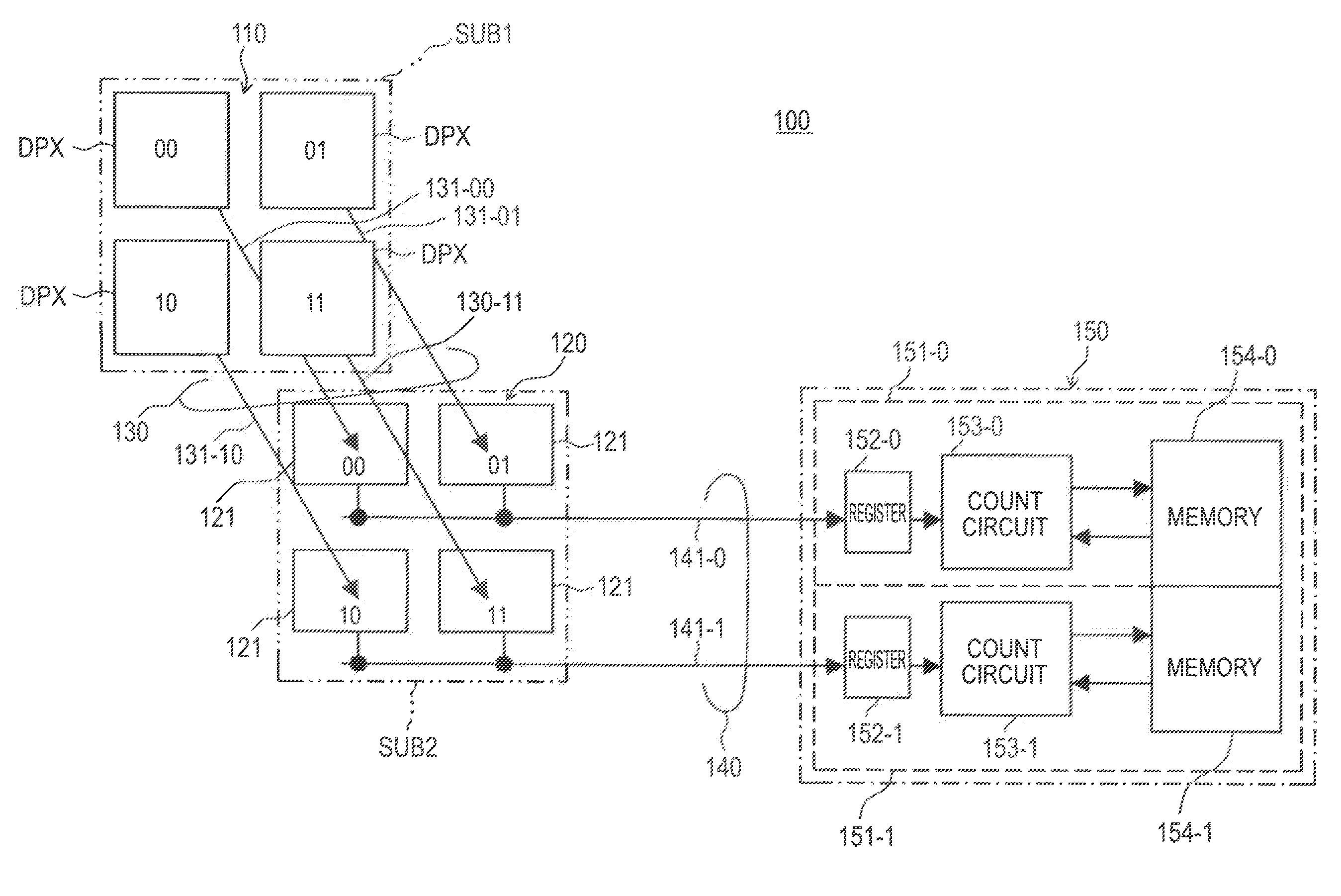
[0111]FIG. 3 is a diagram showing an example of the configuration of a CMOS image sensor (imaging device) 100 according to the first embodiment of the invention.

[Outline of General Configuration]

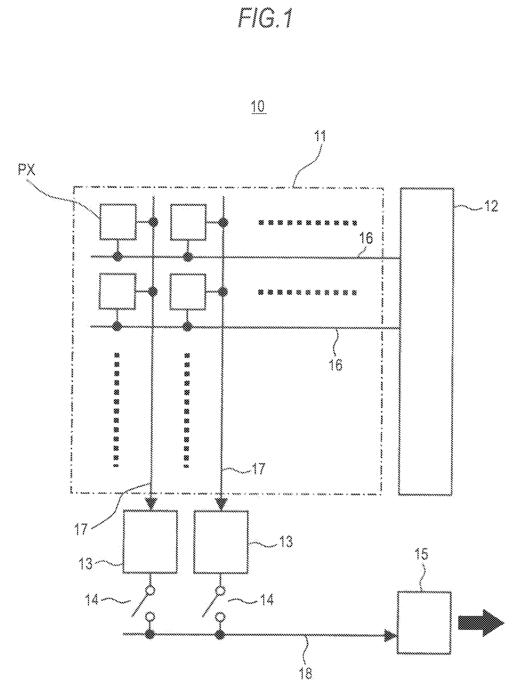
[0112]The CMOS image sensor 100 CMOS image sensor 100 has an pixel array section 110, a sense circuit section 120, a group of output signal lines 130, a group of transfer lines 140, and a decision result IC section 150.

[0113]The pixel array section 110 has a plurality of digital pixels DPX laid out in a matrix form in the row direction and in the column direction.

[0114]Each digital pixel DPX has a photoelectric converting device, and has a function of outputting an electric signal according to an input photon.

[0115]The pixel array section 110 is formed on, for example, a first semiconductor substrate SUB1.

[0116]The sense circuit section 120 is formed on a second semiconductor substrate SUB2 different from the first semiconductor substrate SUB1.

[0117]The sense circuit secti...

second embodiment

3. Second Embodiment

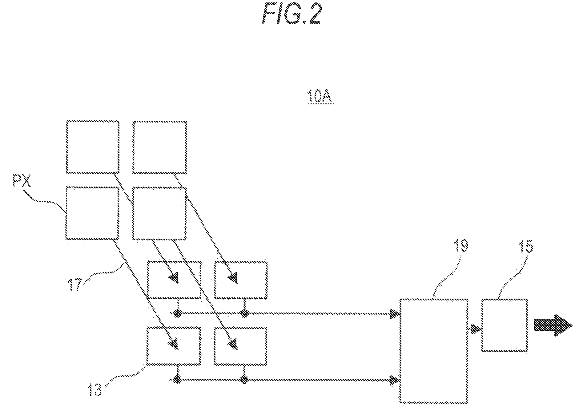
[0223]FIG. 8 is a diagram showing an example of the configuration of a CMOS image sensor (imaging device) according to a second embodiment of the invention.

[0224]In the CMOS image sensor 100 according to the first embodiment, the individual pixels DPX correspond one to one to the sense circuits 121.

[0225]However, the spaces required for the pixels DPX and the sense circuits 121 should not necessarily be the same.

[0226]In addition, with the laminate of two substrates, the count circuits and memories which are large in size may be laid out outside the pixel array region in which fast and long distance transfer of data from each sense circuit 121 is essential, and is likely to be restricted by the layout.

[0227]A CMOS image sensor 100A according to the second embodiment provides a flexible solution to the above problem by allowing a plurality of pixels to share a single sense circuit.

[0228]In the CMOS image sensor 100A, a pixel array section 110A has a plurality of p...

third embodiment

4. Third Embodiment

[0387]FIG. 16 is a diagram showing an example of the configuration of a CMOS image sensor (imaging device) according to a third embodiment of the invention.

[0388]A CMOS image sensor 100B according to the third embodiment has a function of repeatedly executing binary decision on presence / absence of a photon input to a pixel in a predetermined exposure time, multiple times in a unit frame period, and integrating decision results to derive the amount of photons input to the light receiving section.

[0389]The CMOS image sensor 100B also has a function of variably setting the cycle period for decision within a plurality of cycle periods according to N times the unit cycle period (where N is an integer).

[0390]The CMOS image sensor 100B further has a mode of deriving the amount of photons input in the same unit frame period in fewer decisions in a long cycle period, and a mode of deriving the amount of photons input in many decisions in a short cycle period.

[0391]The CMOS...


PUM


Abstract

An imaging device includes: a pixel array section having an array of pixels each of which has a photoelectric converting device and outputs an electric signal according to an input photon; a sense circuit section having a plurality of sensor circuits each of which makes binary decision on whether there is a photon input to a pixel in a predetermined period upon reception of the electric signal therefrom; and a decision result IC section which integrates decision results from the sense circuits, pixel by pixel or for each group of pixels, multiple times to generate imaged data with a gradation, the decision result IC section including a count circuit which performs a count process to integrate the decision results from the sense circuits, and a memory for storing a counting result for each pixel from the count circuit, the plurality of sense circuits sharing the count circuit for integrating the decision results.

Description

BACKGROUND OF THE INVENTION[0001]1. Field of the Invention[0002]The present invention relates to an imaging device like a CMOS image sensor, and a camera system.[0003]2. Description of the Related Art[0004]Recently, CMOS image sensors have widely been used in digital still cameras, camcoders, monitor cameras, etc., and the market for the CMOS image sensors has expanded.[0005]Each pixel in a CMOS image sensor converts input light to electrons using a photodiode which is a photoelectric converting device, stores the electron for a given period, and then outputs a signal reflecting the amount of stored charges to an analog-digital (AD) converter incorporated in a chip. The AD converter digitizes the signal to be sent outside.[0006]The CMOS image sensor has such imaging pixels laid out in a matrix form.[0007]FIG. 1 is a diagram showing the typical chip configuration of a CMOS image sensor 10 which is a solid-state imaging device.[0008]This CMOS image sensor 10 has a pixel array section ...

Claims


Application Information

Patent Timeline
Patent Type & Authority Applications(United States)
IPC IPC(8): H04N5/335
CPCG01J1/44H01L27/14634H01L27/14645H01L27/1469H04N5/3355H04N5/37452H04N5/357H04N5/3537H04N5/359H04N5/361H04N5/365H04N5/3535H01L27/14612H01L27/14621H01L27/14627H01L27/14636H01L27/14643H04N25/772H04N25/533H04N25/60H04N25/79H04N25/00H04N25/62H04N25/63H04N25/67H04N25/75H04N25/76H04N25/534H04N25/771
Inventor NISHIHARA, TOSHIYUKI
Owner SONY CORP
Why Eureka
Try Eureka