Circuit board, semiconductor device including the same, memory module, memory system, and manufacturing method of circuit board

a technology of circuit board and semiconductor device, which is applied in the direction of electrical apparatus construction details, electrical apparatus casings/cabinets/drawers, instruments, etc., can solve the disadvantages of contact reliability of memory module with socket, the number of terminals to be provided on a memory module may reach a number that cannot, and the reduction of pitch and the so as to achieve reliable electric connection and sufficient pitch and width of board terminals

Inactive Publication Date: 2011-03-03
ELPIDA MEMORY INC
View PDF6 Cites 13 Cited by
  • Summary
  • Abstract
  • Description
  • Claims
  • Application Information

AI Technical Summary

Benefits of technology

[0010]According to the present invention, because board terminals are provided not only on the main surface but also on a side surface of the circuit board, the total number of the board terminals can be increased while maintaining sufficient pitch and width of the board terminals. Furthermore, the board terminals that are provided on the side surface are formed by not only exposing the internal wiring, but by covering the side surface of the circuit board with the board terminals. As a result, in contrast to the semiconductor device described in Japanese Patent Application Laid-open No. 2006-324326, reliable electric connection can be achieved.

Problems solved by technology

Therefore, there has been a concern that the number of terminals to be provided on a memory module may reach a number that cannot be accommodated within the area that has been set by the standards.
However, the contact reliability of the memory module with the socket disadvantageously decreases when the pitch and the width of the board terminals is decreased.
The above problem is not limited to memory modules, and the same problem arises in circuit boards having board terminals and semiconductor devices including the circuit board.

Method used


Image

  • Circuit board, semiconductor device including the same, memory module, memory system, and manufacturing method of circuit board
  • Circuit board, semiconductor device including the same, memory module, memory system, and manufacturing method of circuit board
  • Circuit board, semiconductor device including the same, memory module, memory system, and manufacturing method of circuit board

Examples


first embodiment

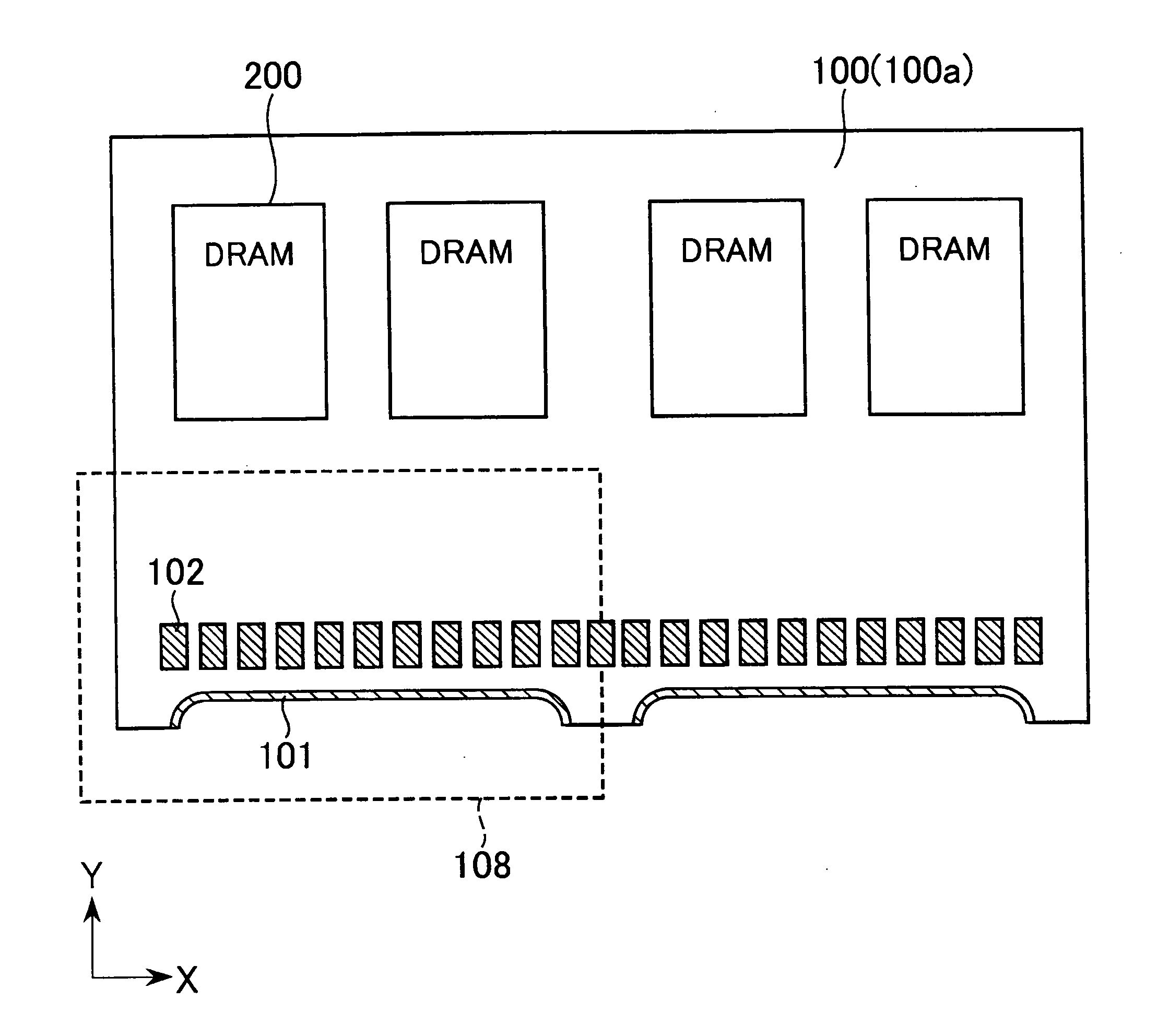
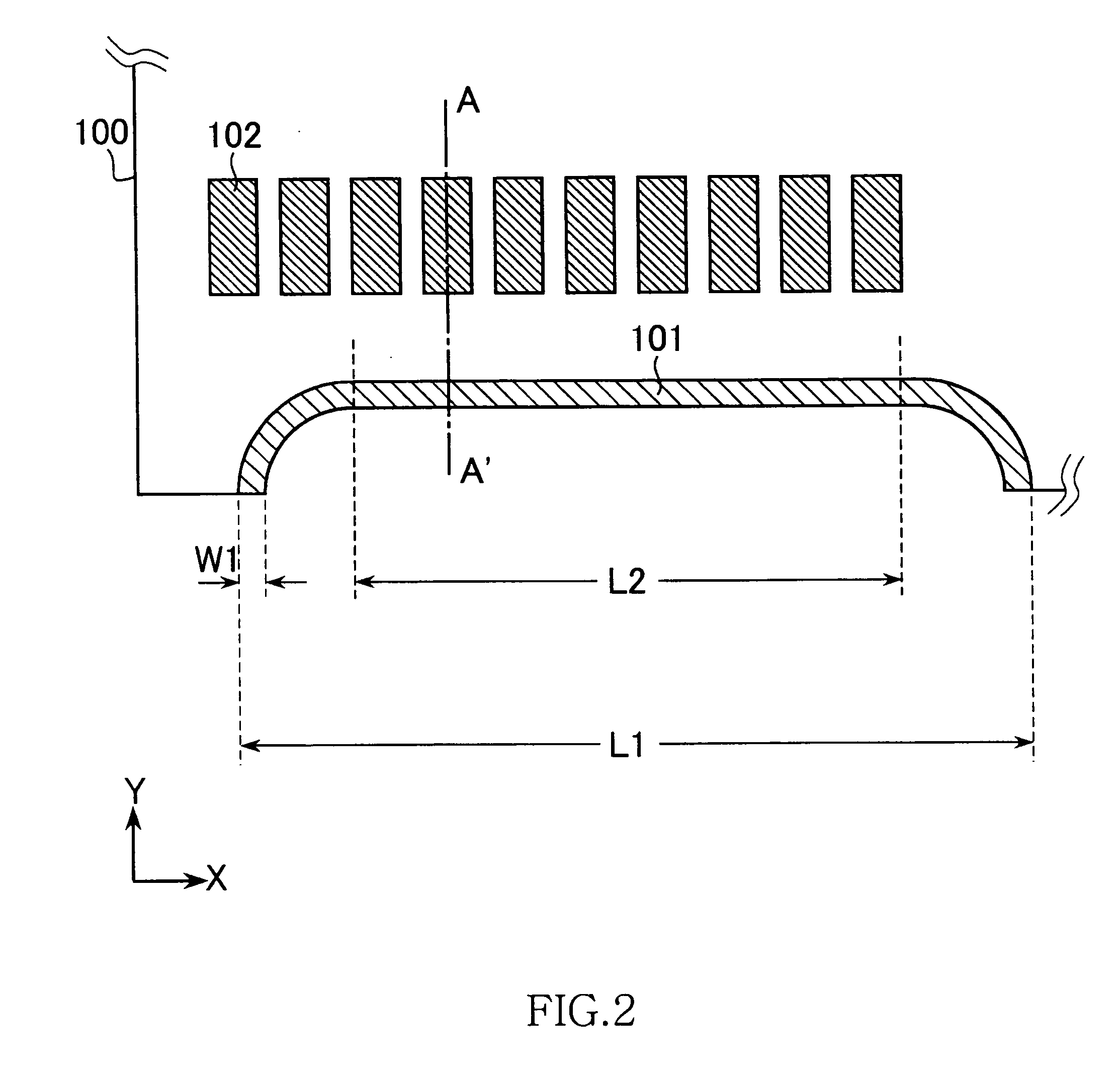
[0023]FIG. 1 is a schematic plan view of a configuration of a memory module according to the present invention.

[0024]The memory module according to the first embodiment is a so-called SO-DIMM, and more specifically it is a semiconductor device in which a plurality (four in this example) of DRAMs 200 are mounted on a main surface 100a of a module board (a circuit board) 100. It is needless to say that the target of the present invention is not limited to SO-DIMMs, and the present invention can be also applied to various types of DIMMs (including Unbuffered-DIMM or FB-DIMM). Moreover, the semiconductor chip to be mounted is not limited to the DRAM, but can be other semiconductor memories (such as a SRAM, a flash memory, and a PRAM). Furthermore, the semiconductor chip to be mounted on the circuit board does not need to be a memory, but can be a device such as a CPU or a microcomputer.

[0025]The main surface 100a of the module board 100 is substantially rectangular with a long side exte...

second embodiment

[0047]FIG. 8 is a schematic plan view of a configuration of a memory module according to the present invention.

[0048]As shown in FIG. 8, in the second embodiment, four board terminals 101 are provided on the side surface. Among the four board terminals 101, a board terminal 101-V1 is a terminal for providing the power potential VDD to DRAMs 200-1 and 200-2 and a board terminal 101-G1 is a terminal for providing the ground potential GND to the DRAMs 200-1 and 200-2. On the other hand, a board terminal 101-V2 is a terminal for providing the power potential VDD to DRAMs 200-3 and 200-4 and a board terminal 101-G2 is a terminal for providing the ground potential GND to the DRAMs 200-3 and 200-4.

[0049]In this manner, in the second embodiment, a plurality of the DRAMs 200 are divided into groups and the power terminals are allocated per group. With this configuration, it is possible to make the power supply efficiency uniform for each of the DRAMs 200. It is needless to say that the power...

third embodiment

[0050]FIGS. 9A and 9B show a configuration of a memory module according to the present invention, where FIG. 9A is a schematic perspective view of the memory module and FIG. 9B is a cross-sectional view of the memory module taken along a line B-B′ shown in FIG. 9A.

[0051]As shown in FIGS. 9A and 9B, in the third embodiment, three board terminals 101 are provided on the side surface. Among the three board terminals 101, board terminals 101-G1 and 101-G2 arranged on either sides are the terminals to which the ground potential GND is supplied and a board terminal 101-V arranged in between is a terminal to which the power potential VDD is supplied. Within the module board 100, as shown in FIG. 9B, a wide ground wiring 301G and a plurality of data wirings 302DQ are provided along each other so as to overlap in a laminating direction (the Z direction) of the module board 100 and, similarly, a wide VDD wiring 301V and a plurality of command address wirings 302CA are provided along each othe...


PUM


Abstract

A circuit board according to the present invention includes a main surface, a back surface parallel to the main surface, a side surface positioned between edges of the main surface and the back surface, and first and second board terminals covering a portion of the main surface and a portion of the side surface, respectively. According to the present invention, because the board terminals are provided not only on the main surface but also on the side surface of the circuit board, the total number of board terminals can be increased while maintaining sufficient pitch and width of the board terminals.

Description

BACKGROUND OF THE INVENTION[0001]1. Field of the Invention[0002]The present invention relates to a circuit board and a semiconductor device including the circuit board, and more particularly relates to a circuit board in which it is possible to reduce the number of board terminals to be formed on a main surface, and a semiconductor device including the circuit board. The present invention also relates to a memory module and a memory system including the circuit board and a manufacturing method of the circuit board.[0003]2. Description of Related Art[0004]DRAM (Dynamic Random Access Memory) is widely used as a main memory in personal computers and servers. In a personal computer or a server, instead of mounting a DRAM directly on a motherboard, it is a common to attach the DRAM to a socket (a memory slot) provided on the motherboard in the form of a memory module mounted onto a module board (see Japanese Patent Application Laid-open No. 2006-324326).[0005]In recent years, the amount ...

Claims


Application Information

Patent Timeline
Patent Type & Authority Applications(United States)
IPC IPC(8): G06F1/16H01R12/30H05K7/02
CPCH05K1/0263H05K1/0298H05K1/117H05K3/0052H01R12/721H05K2201/09172H05K2201/09181H05K2201/0919H05K2201/09345H05K3/403
Inventor HARASHIMA, SHIRO
Owner ELPIDA MEMORY INC
Why Eureka
Try Eureka