

Method for modifying insulating film with plasma
a technology of insulating film and plasma, which is applied in the direction of electric discharge tubes, semiconductor devices, solid-state devices, etc., can solve the problems of incompatible demand for reducing the amount of thermal treatment, difficult to suppress the leakage current, and insufficient quality of silicon oxide film formed with low-temperature cvd method, etc., to suppress the amount of heat treatment and plasma damage, suppress the leakage current, and high quality
- Summary
- Abstract
- Description
- Claims
- Application Information
AI Technical Summary
Benefits of technology
Problems solved by technology
Method used
Image

Examples
first embodiment
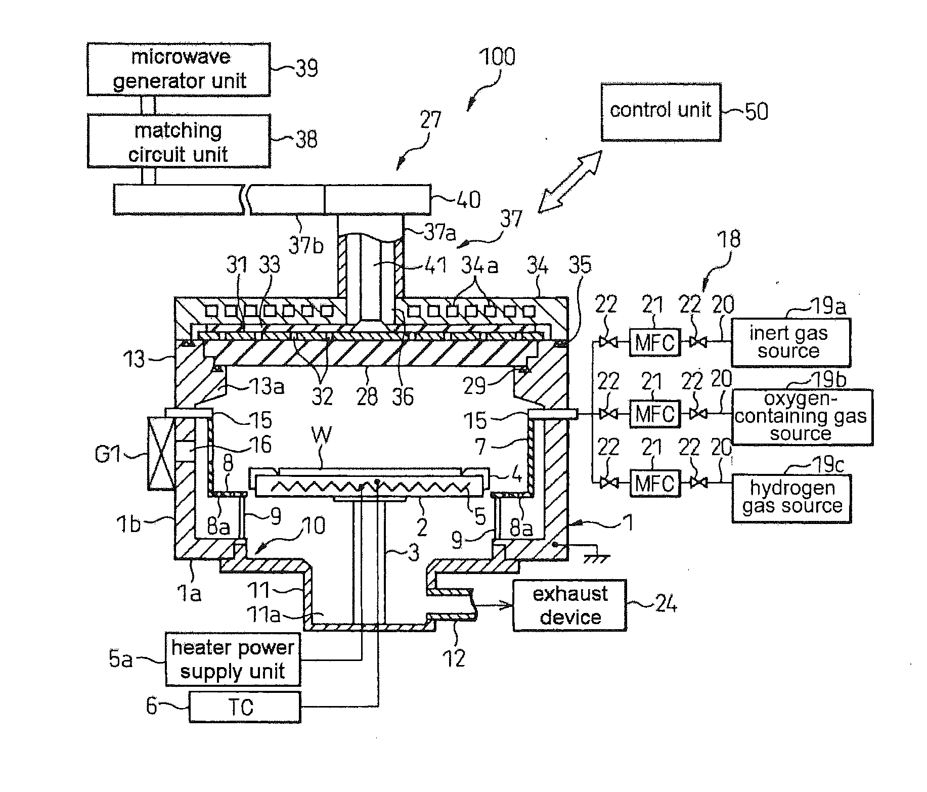
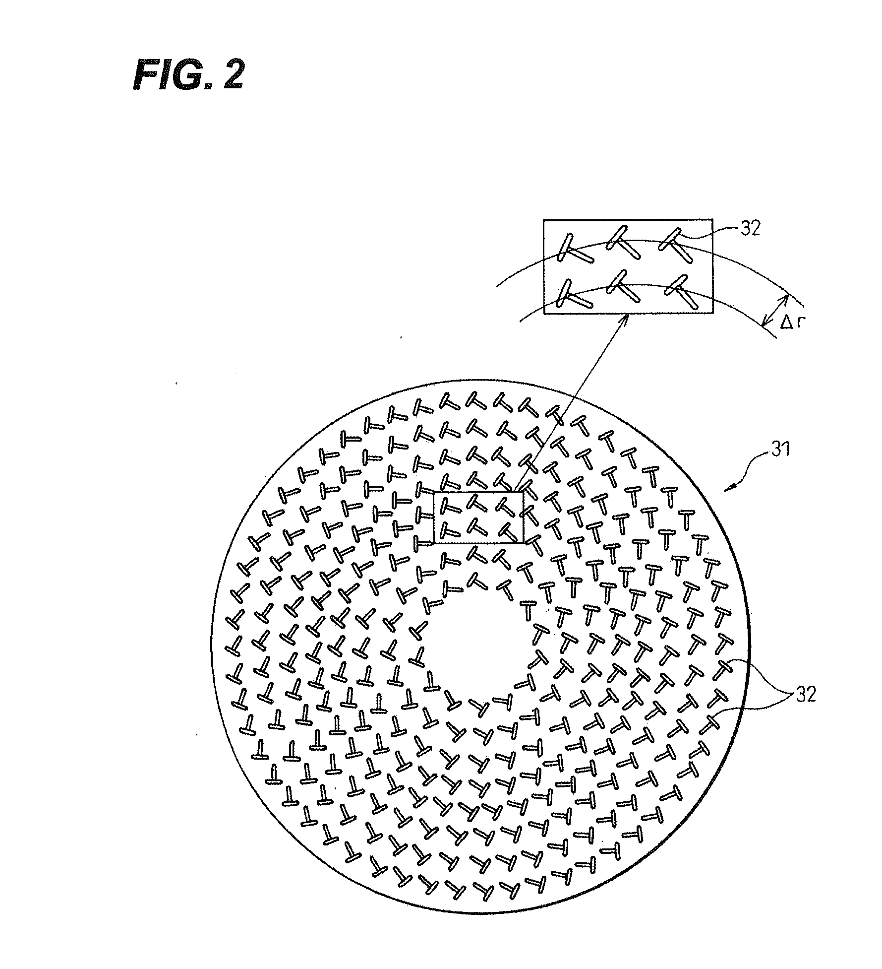
[0041]Hereinafter, embodiments of the present invention will be described in detail with reference to the accompanying drawings which form a part hereof. First of all, FIG. 1 is a cross-sectional view illustrating mimetically a schematic constitution of a plasma processing apparatus 100 applicable to the plasma modification process according to present embodiment. Also, FIG. 2 is a plan view illustrating the plane antenna of plasma processing apparatus 100 shown in FIG. 1.
[0042]Plasma processing apparatus 100 is constituted with a Radial Line Slot Antenna (RLSA) microwave plasma processing apparatus capable of generating a high density and low temperature microwave-excited plasma by introducing microwave into a processing chamber through a plane antenna having a plurality of slot-type holes, specifically, the RLSA. Because it is possible to process with plasma having a density of 1×10¹⁰ to 5×12 / cm2 and the low electron temperature of 0.7 to 2 eV, there is no plasma damage in plasma ...
second embodiment
[0174]Next, the plasma modifying method according to the second embodiment of the present invention will be explained with reference to FIGS. 16 through 20. FIG. 16 is a flowchart showing an exemplary flow of the plasma modifying method according to the second embodiment of the present invention. In the above first embodiment, the plasma modification process is performed under the low pressure condition of below 267 Pa, for example, 6.7 Pa to 267 Pa, thereby modifying the silicon oxide film formed with the CVD method to a high quality film being dense and having fewer impurities. However, in the present embodiment, it is constituted that prior to the plasma modification process under the low pressure condition, the plasma modification process is performed under a high pressure condition using plasma modifying apparatus 100.
[0175]In FIG. 16, a wafer (W) formed with a silicon oxide film as an insulating film is carried into plasma modifying apparatus 100 at first. Next, in step S12, p...
PUM
| Property | Measurement | Unit |
|---|---|---|
| temperature | aaaaa | aaaaa |
| pressure | aaaaa | aaaaa |
| pressure | aaaaa | aaaaa |
Abstract
Description
Claims
Application Information