
Method of producing piezoelectric/electrostrictive film type device

a piezoelectric/electrostrictive film and film type technology, applied in the direction of piezoelectric/electrostrictive/magnetostrictive devices, printing, electrical transducers, etc., can solve the problem of limited plane position of the lowermost electrode film from the plane position of the cavity, and achieve the effect of increasing the coating ratio improving the heat resistance of the lowermost electrode film

Inactive Publication Date: 2011-03-10
NGK INSULATORS LTD
View PDF5 Cites 8 Cited by
  • Summary
  • Abstract
  • Description
  • Claims
  • Application Information

AI Technical Summary

Benefits of technology

[0011]It is an object of the present invention to increase the coating ratio of the lowermost electrode film and to prevent the deviation of the plane position of the lowermost electrode film from the plane position of the cavity.
[0013]This method improves the packing density of the lowermost electrode film and also, improves the heat resistance and therefore, the coating ratio of the lowermost electrode film is increased. Further, since the lowermost electrode film is formed in the region where the cavity is formed, the deviation of the plane position of the lowermost electrode film from the plane position of the cavity is limited.
[0015]This method improves the heat resistance of the lowermost electrode film and therefore, the coating ratio of the lowermost electrode film is increased. Further, since the lowermost electrode film is formed in the region where the cavity is formed, the deviation of the plane position of the lowermost electrode film from the plane position of the cavity is limited.
[0017]This method improves the heat resistance of the lowermost electrode film and therefore, the coating ratio of the lowermost electrode film is increased. Further, since the lowermost electrode film is formed in the region where the cavity is formed, the deviation of the plane position of the lowermost film from the plane position of the cavity is limited. Moreover, since the lowermost electrode film is repelled by the water-repellent film, the end tail projection at the end of the lowermost electrode film is limited.
[0019]This method improves the heat resistance of the lowermost electrode film and therefore, the coating ratio of the lowermost electrode film is increased. Further, since the lowermost electrode film is formed in the region where the cavity is formed, the deviation of the plane position of the lowermost film from the plane position of the cavity is limited. Moreover, since the lowermost electrode film is repelled by the water-repellent film, the end tail projection at the end of the lowermost electrode film is limited.

Problems solved by technology

Further, since the lowermost electrode film is formed in the region where the cavity is formed, the deviation of the plane position of the lowermost electrode film from the plane position of the cavity is limited.

Method used


Image

  • Method of producing piezoelectric/electrostrictive film type device
  • Method of producing piezoelectric/electrostrictive film type device
  • Method of producing piezoelectric/electrostrictive film type device

Examples


first preferred embodiment

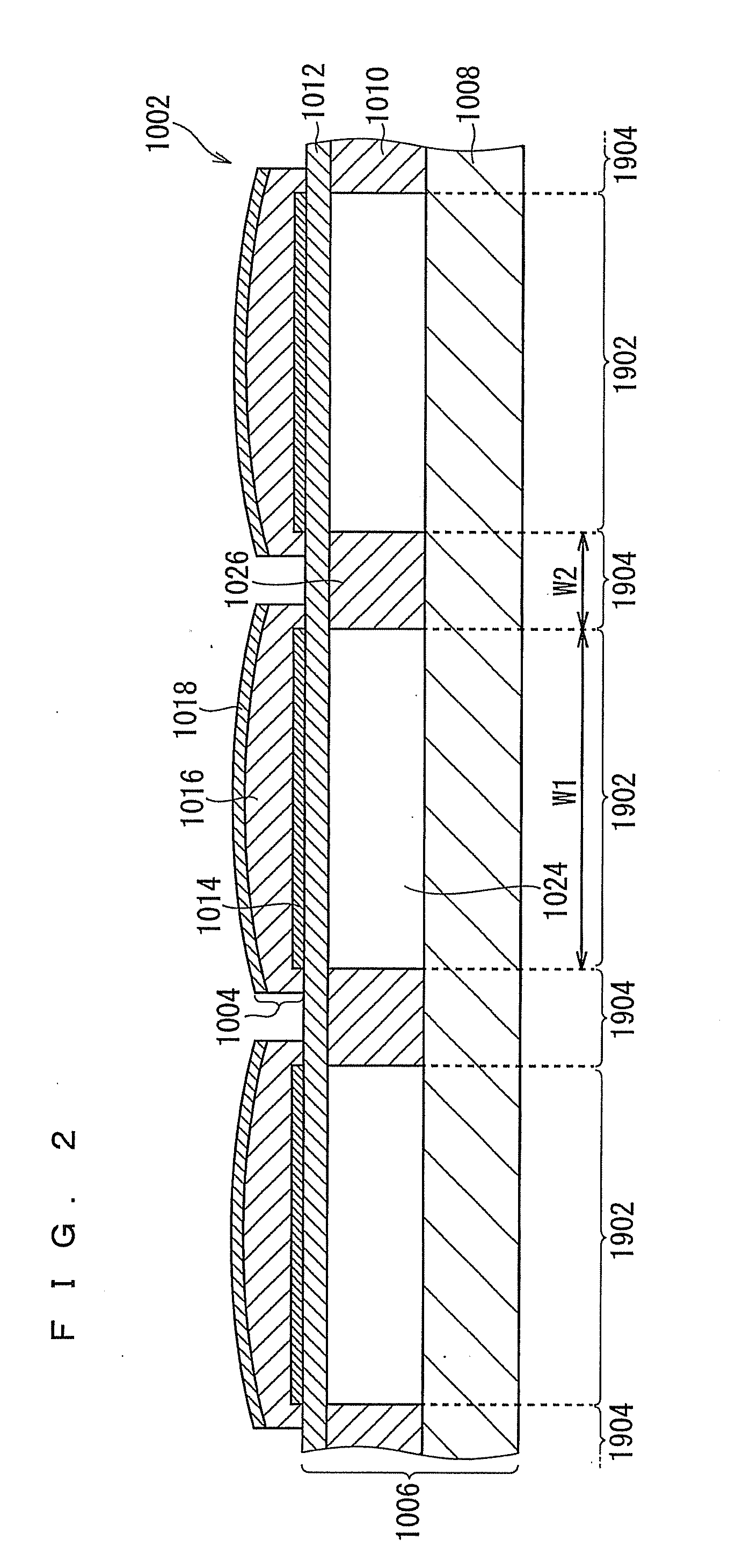
[0036]In a first preferred embodiment, which relates to a method of producing a piezoelectric / electrostrictive film type device provided with a substrate formed with a cavity and an vibrating laminate obtained by laminating a lower electrode film, a piezoelectric / electrostrictive film, an upper electrode film which are aligned with the plane position of the cavity, on the surface of the substrate, the lower electrode film is formed by using, as a mask, the substrate in which the cavity is filled with a light-shielding agent according to photolithography. Thereafter, a powder of piezoelectric / electrostrictive material is made to flow towards the lower electrode film by electrophoresis to form a piezoelectric / electrostrictive film and then, an upper electrode film is formed using the piezoelectric / electrostrictive material as a mask according to the photolithography.

[0037]1002>

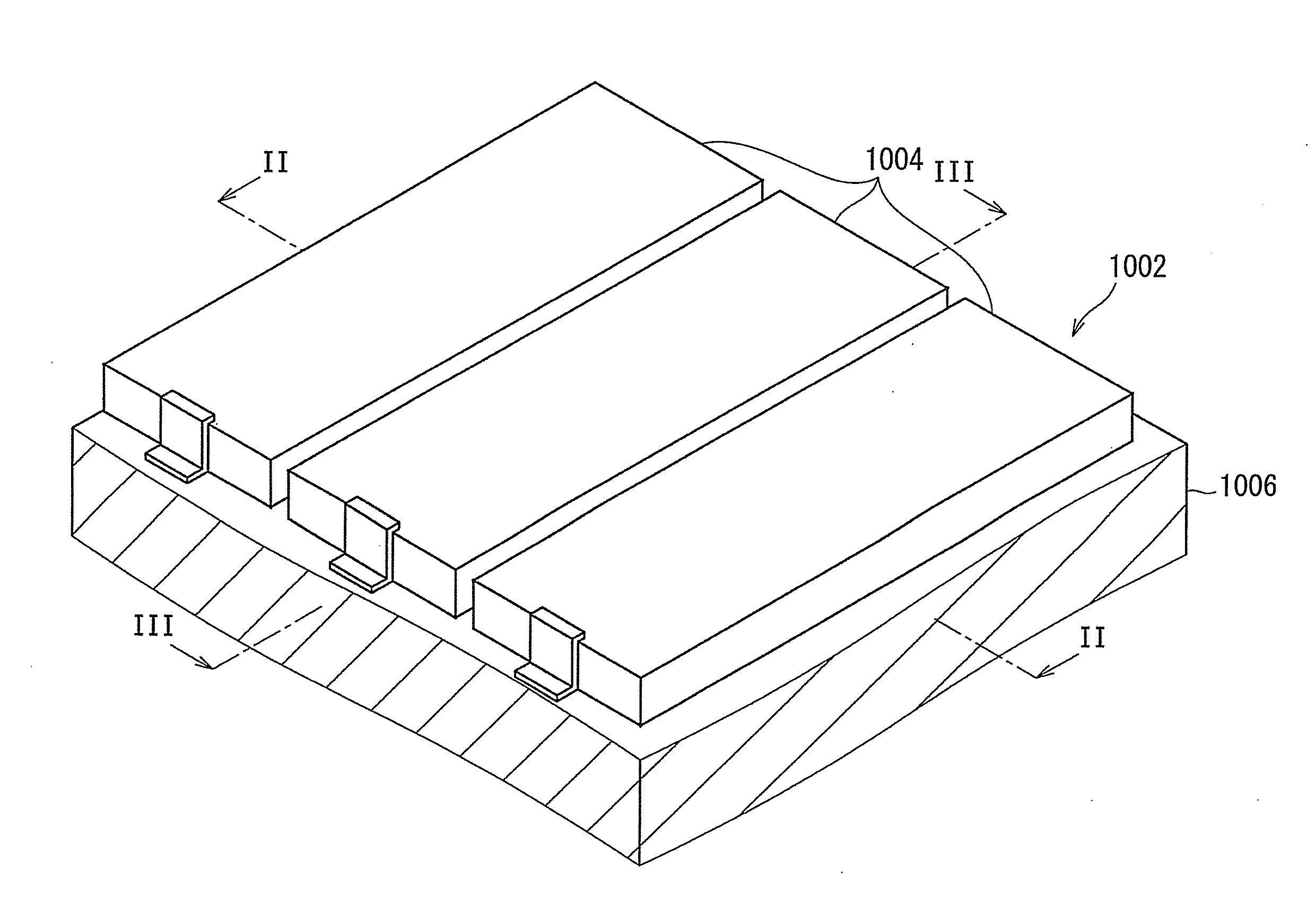
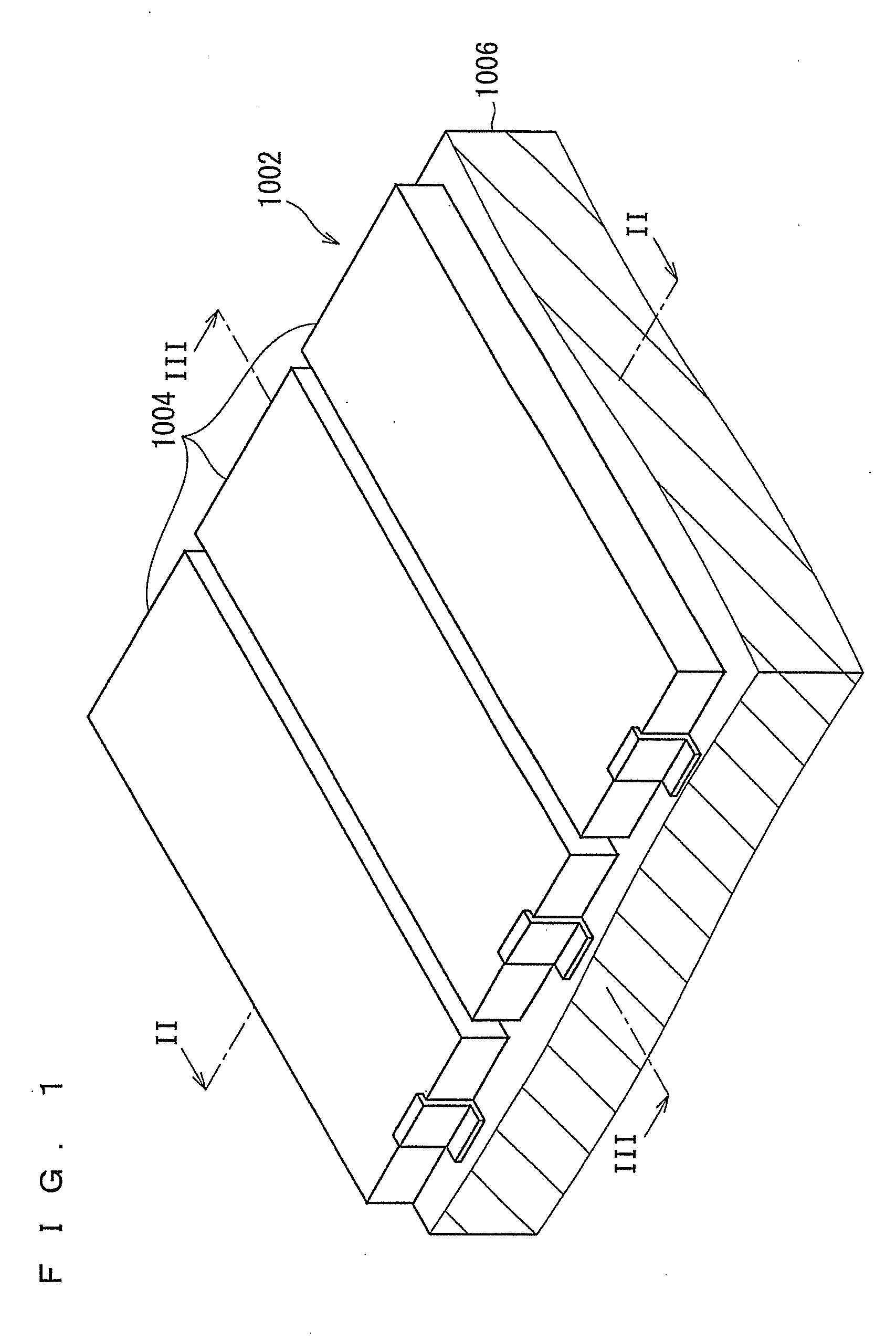
[0038]FIGS. 1 to 3 are schematic views each showing a outline structure of a piezoelectric / electrostrictive f...

fifth preferred embodiment

[0143]A fifth preferred embodiment relates to treatment (hereinafter referred to as “projection limiting treatment”) for limiting the end tail projection at the end of the lower electrode film 1014 which treatment is preferably carried out after the resist film pattern 1042 according to the first preferred embodiment is formed (FIG. 4) and before the catalyst pattern 1044 is formed (FIG. 5). This projection limiting treatment is preferably carried out also in the case of adopting the resist film pattern 4042 of the fourth preferred embodiment instead of the resist film pattern 1042 of the first preferred embodiment. The projection limiting treatment according to the fifth preferred embodiment is preferably adopted in the case where the contact angle of the conductive material with the resist film pattern 1042 or 4042 cannot be increased in the first or fourth preferred embodiment.

[0144]FIGS. 46 to 49 are views for describing the projection limiting treatment in the fifth preferred e...

experiment 1

8.1 Experiment 1

[0162]In Experiment 1, a lower electrode film 1014 was formed on the surface of the substrate 1006 according to the procedures described in the first preferred embodiment.

[0163]In the process of forming the resist film 1056, a resist solution was applied to the surface of the substrate 1006 by a spin coater and the half-finished product was heated by a hot plate to vaporize a solvent from the coating film. When the resist solution was applied, the number of rotations of the spin coater was set to 1000 rpm and the rotation holding time was set to 6 sec. When the solvent was vaporized, the temperature was set to 100° C. and the heating time was set to 3 min. As the resist solution, a polyimide coating agent having a solid content of 19% by weight was used. The film thickness of the formed resist film pattern 1042 was 6.5 μm.

[0164]In the process of filling the light-shielding agent 1058, a light-shielding solution was injected into the cavity 1024 from the ink jetting h...


PUM

PropertyMeasurementUnit
Thicknessaaaaaaaaaa
Adhesion strengthaaaaaaaaaa
Piezoelectricityaaaaaaaaaa

Abstract

Provided is a method of producing a piezoelectric / electrostrictive film type device, the method making it possible to increase the coating ratio of the lowermost electrode film and also, to prevent the deviation of the plane position of the lowermost electrode film from the plane position of the cavity. In the production of a piezoelectric / electrostrictive film provided with a substrate formed with a cavity and an vibrating laminate obtained by laminating a lower electrode film, a piezoelectric / electrostrictive film and an upper electrode film which are aligned with the plane position of the cavity, on the surface of the substrate, the lower electrode film is formed using, as a mask, the substrate in which a light-shielding agent is filled in the cavity by photolithography. The lower electrode film is formed by electroless plating after the catalyst layer is formed.

Description

BACKGROUND OF THE INVENTION[0001]1. Field of the Invention[0002]The present invention relates to a method of producing a piezoelectric / electrostrictive film type device provided with a substrate formed with a cavity and a vibrating laminate obtained by laminating electrode films and a piezoelectric / electrostrictive film which are aligned with the plane position of the cavity, on a first principal surface of the substrate.[0003]2. Description of the Background Art[0004]FIGS. 58A to 58C are schematic sectional views for describing a conventional method of producing a piezoelectric / electrostrictive film type device 9 constituting the essential part of an ink jetting piezoelectric / electrostrictive actuator to be used for the head of an ink jet printer.[0005]In the conventional production method, as shown in FIG. 58A, a conductive material paste is applied by screen printing to the surface of a substrate 902 formed with a cavity 926 which is to be an ink pressure room and the obtained co...

Claims


Application Information

Patent Timeline
IPC IPC(8): H01L41/22H01L41/29H01L41/314H01L41/39
CPCB41J2/161Y10T29/42B41J2/1629B41J2/1631B41J2/1632B41J2/1642B41J2/1643B41J2/1645B41J2/1646H01L41/0973H01L41/29H01L41/314Y10T29/49155Y10T29/49128B41J2/1628H10N30/2047H10N30/06H10N30/077H10N30/074
Inventor SHIMIZU, HIDEKIKITAGAWA, MUTSUMI
Owner NGK INSULATORS LTD
Learn More