Method for the real-time monitoring of integrated circuit manufacture through localized monitoring structures in opc model space

a technology of integrated circuits and local monitoring structures, applied in the field of manufacturing of integrated circuits, can solve the problems of significant gain in the development cycle time, and achieve the effects of increasing the validation rate, reducing the number of unreliable solutions, and increasing the removal rate of unreliable solutions

Active Publication Date: 2011-03-10
STMICROELECTRONICS (ROUSSET) SAS
View PDF2 Cites 10 Cited by
  • Summary
  • Abstract
  • Description
  • Claims
  • Application Information

AI Technical Summary

Benefits of technology

[0025]Thus, it is possible to monitor the changes of the entire model on each semiconductor wafer being processed while ensuring that if the control pattern is correct, the other patterns formed on the wafer are correct. The constitution of a control pattern also enables a model derived from another previously validate

Problems solved by technology

The result is a significant gai

Method used


Image

  • Method for the real-time monitoring of integrated circuit manufacture through localized monitoring structures in opc model space
  • Method for the real-time monitoring of integrated circuit manufacture through localized monitoring structures in opc model space
  • Method for the real-time monitoring of integrated circuit manufacture through localized monitoring structures in opc model space

Examples


Embodiment Construction

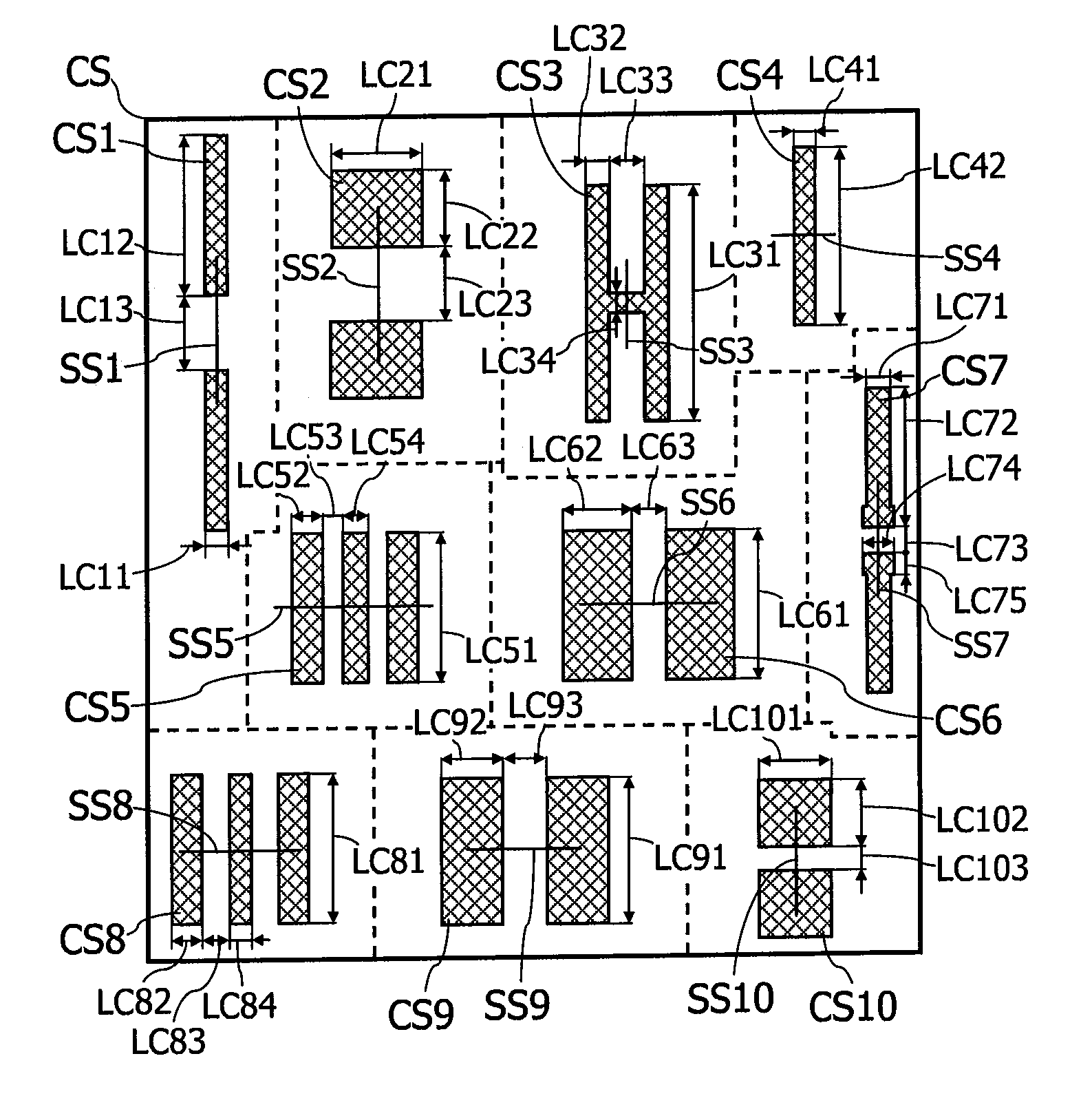
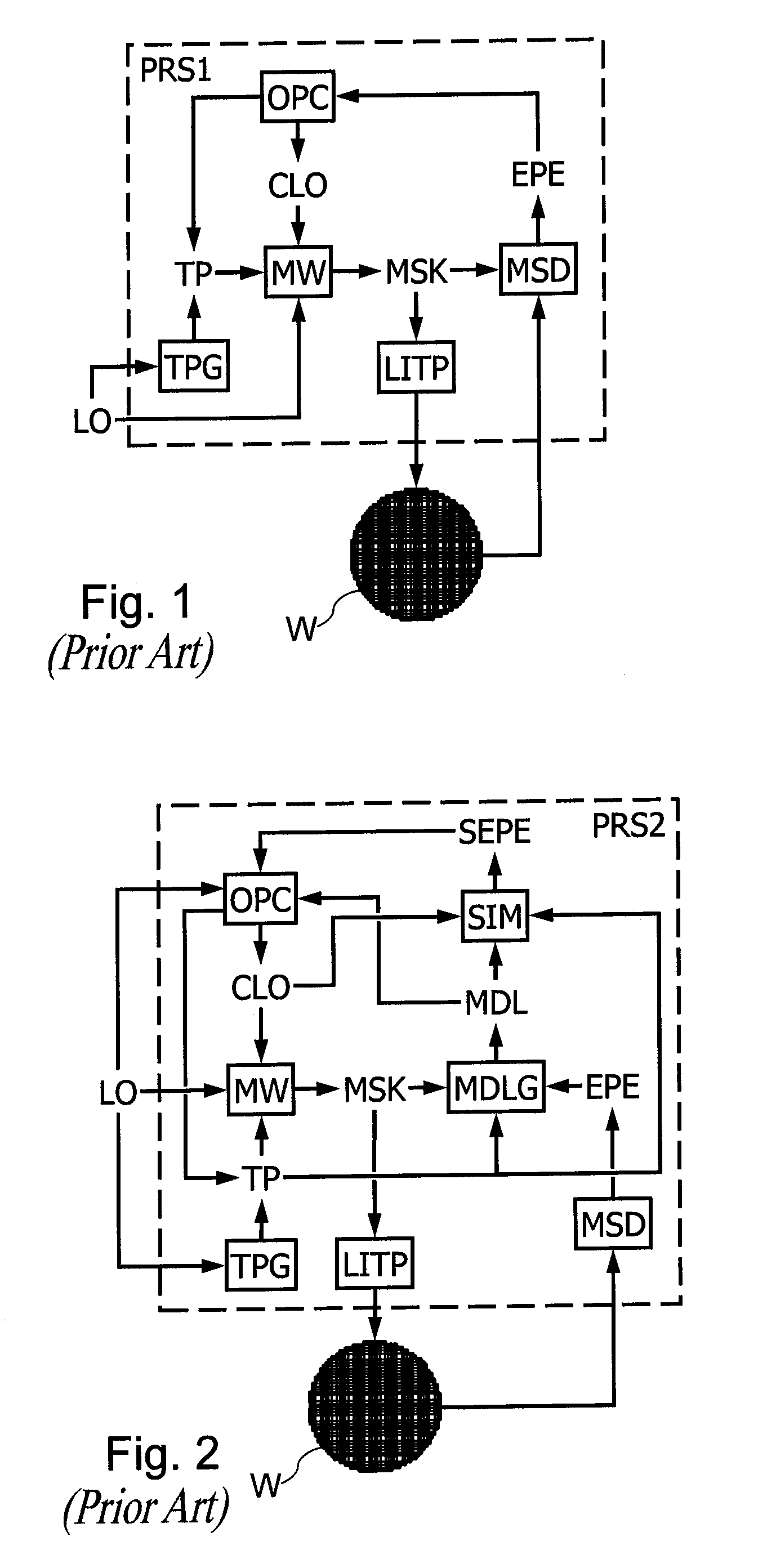
[0055]FIG. 6 represents steps of a control method PRS3 according to one embodiment. In FIG. 6, the method comprises a step of generating CSG control structures CS using a mask layout LO and a model MDL. The control structures are generated so as to be more sensitive to drifts of manufacturing parameters than the integrated circuit structures to be formed on a semiconductor wafer W. During a next step MW, a mask MSK is generated from the control structures CS and the layout LO. Then there is a lithography step LITP possibly followed by an etching step to transfer the mask MSK to a resist layer previously deposited on a semiconductor wafer W. During a next step MSD, measurements are taken on the wafer W so as to assess the features MS of the control structures CS transferred to the wafer. If the features obtained are not satisfactory, a new generation and validation cycle is performed to change one or more of the control structures (step CSG), to transfer them to a wafer W (steps MW, ...


PUM


Abstract

The present disclosure relates to a method of controlling the manufacturing of integrated circuits, comprising steps of determining parameters that are characteristic of a curve of radiation intensity applied to a semiconductor wafer through a mask, in critical zones of structures to be formed on the wafer, for each of the critical zones, placing a measuring point in a multidimensional space each dimension of which corresponds to one of the characteristic parameters, placing control points in the multidimensional space that are spread around an area delimited by the measuring points, so as to delimit an envelope surrounding the area, for each control point, defining control structures each corresponding to a control point, generating a mask containing the control structures, applying a process involving the generated mask to a semiconductor wafer, and analyzing the control structures transferred to the wafer to detect any defects therein.

Description

BACKGROUND[0001]1. Technical Field[0002]The present disclosure relates to the manufacturing of integrated circuits. The present disclosure relates more particularly to controlling the different processes which are applied to the semiconductor wafers during the manufacturing of integrated circuits, and particularly the lithography, etching, polishing and planarization processes. The present disclosure also relates to the validation of the masks used during the lithography processing.[0003]2. Description of the Related Art[0004]A lithography process classically comprises steps of depositing a resist layer made of light-sensitive resin onto a wafer made of a semi-conductive material, and of exposing the resist layer through a mask, to radiation (visible light, ultraviolet light, X rays, beam of electrons, etc.). The resist layer exposed to the radiation is then developed so as to form a mask on the wafer. The wafer and the mask formed in the resist layer may then be subjected to an etc...

Claims


Application Information

Patent Timeline
IPC IPC(8): H01L23/544G06F17/50G03F1/00
CPCG03F7/70483G03F1/144G03F1/00G03F1/36
Inventor DI GIACOMO, ANTONIOSABATIER, ROMUALD
Owner STMICROELECTRONICS (ROUSSET) SAS
Why Eureka
Try Eureka