
Electromagnetic based thermal sensing and imaging

a technology of electromagnetic radiation and thermal sensing, applied in the field of electromagnetic radiation based thermal sensing and imaging, can solve the problems of low sensitivity, high cost of sensor manufacture, and need cryogenic cooling to 77° k, and achieve the effect of potentially higher sensitivity of thermal sensors

Inactive Publication Date: 2011-03-17
ORYX VISION LTD
View PDF6 Cites 31 Cited by
  • Summary
  • Abstract
  • Description
  • Claims
  • Application Information

AI Technical Summary

Benefits of technology

[0014]Use of the electromagnetic approach to thermal imaging and the resultant pixel circuit of the invention provides numerous advantages, including (1) no cooling of the thermal sensor is required since the noise figure of the system is almost constant over temperature; (2) no MEMS technology is required as the pixel circuit is fabricated on a monolithic semiconductor substrate using standard IC processes; (3) no vacuum packaging is required as is the case with prior art thermal sensors; and (4) the sensitivity of the thermal sensor is potentially higher than of uncooled sensors, because detection is performed directly on the received signal, rather than on a signal from a second-stage conversion.

Problems solved by technology

A major disadvantage, however, is that these sensors arc very expensive to manufacture.
Another disadvantage is that they require cryogenic cooling to 77° K, for example, to function well.
A disadvantage of uncooled imagers, however, it that they typically exhibit low sensitivity, and also require complex, expensive and difficult to construct Micro Electro Mechanical Systems (MEMS) production technologies.
Furthermore, they require vacuum packaging to work well which is required to thermally isolate one pixel from the adjacent pixels.

Method used


Image

  • Electromagnetic based thermal sensing and imaging
  • Electromagnetic based thermal sensing and imaging
  • Electromagnetic based thermal sensing and imaging

Examples


example unbalanced

Pixel Circuits

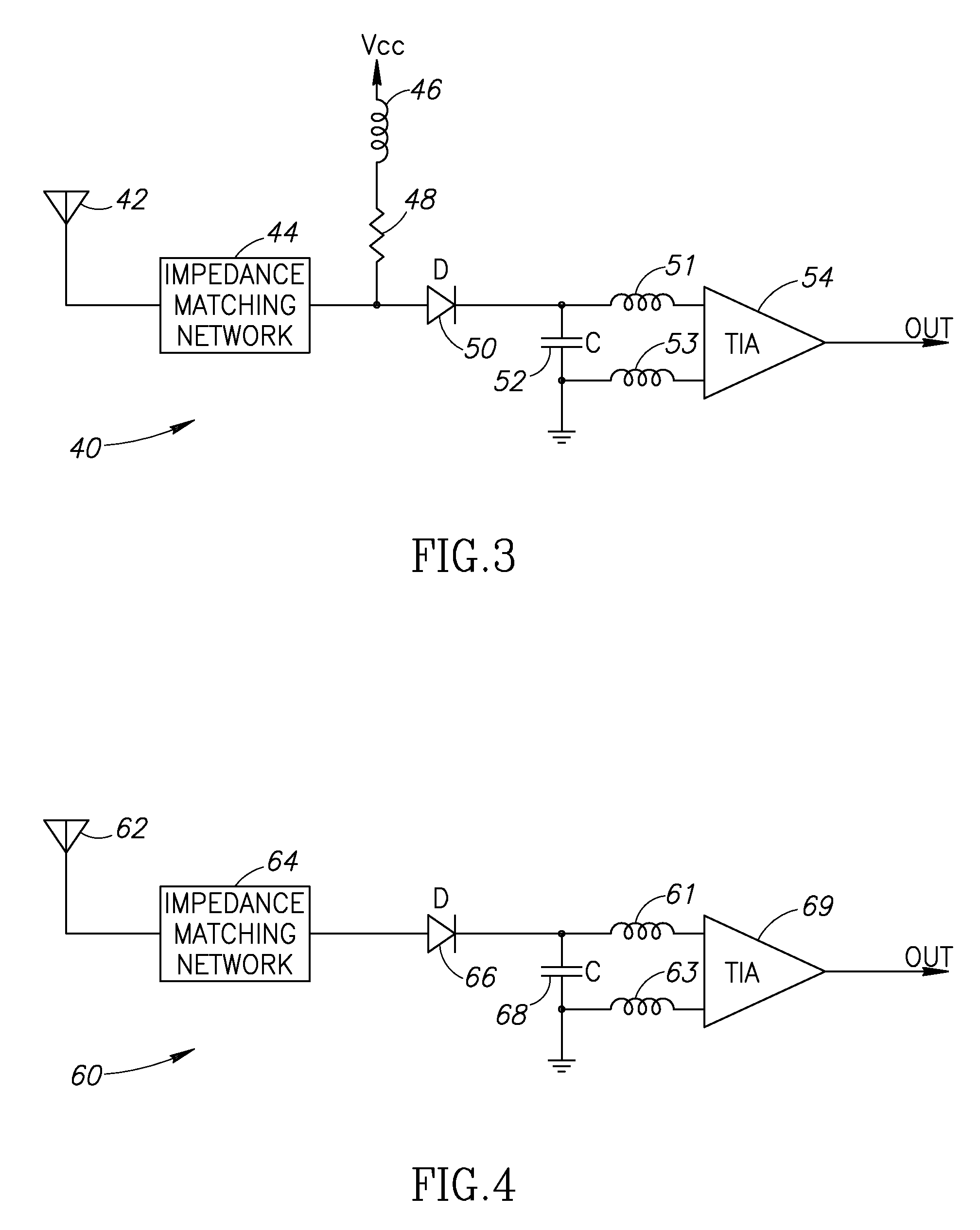
[0138]Several example pixel circuits are presented infra to aid in illustrating the possible variations of the pixel circuit of the present invention. Four example pixel circuits are shown illustrating unbalanced, biased and unbiased, and voltage and current sense topologies. It is appreciated that the present invention is not limited to the example pixel circuits presented herein as one skilled in the electrical art can construct other circuit topologies in accordance with the principles of the invention.

[0139]A schematic diagram illustrating an example balanced, biased topology, current sense pixel circuit is shown in FIG. 19. The thermal pixel circuit, generally referenced 300, comprises a high frequency front end sensor circuit portion 302 and a low frequency back end readout circuit portion 304. The front end circuit sensor circuit comprises an antenna 306, transformer T / impedance matching network, series capacitor C4 tied to series combination of capacitor C1, re...


PUM


Abstract

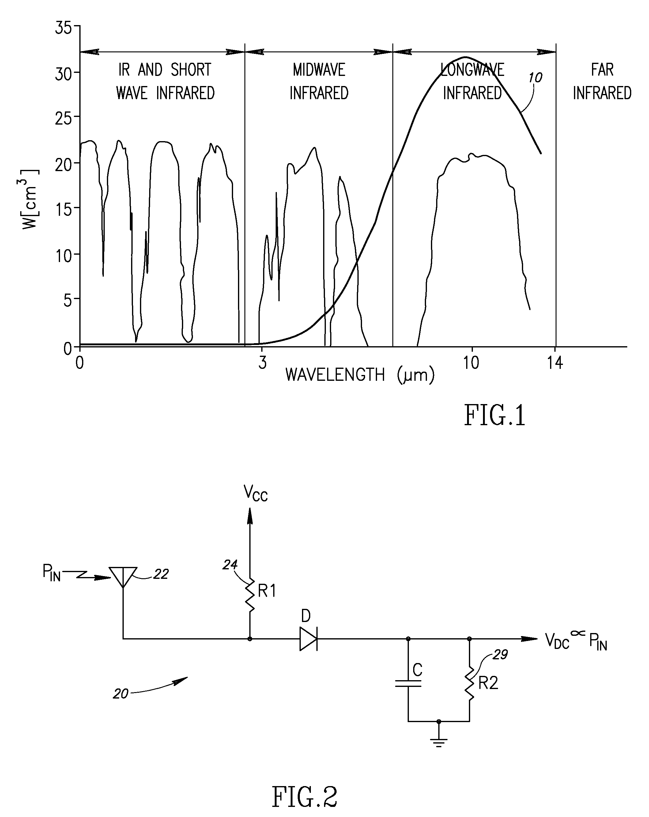
A novel pixel circuit and multi-dimensional array for receiving and detecting black body radiation in the SWIR, MWIR or LWIR frequency bands. An electromagnetic thermal sensor and imaging system is provided based on the treatment of thermal radiation as an electromagnetic wave. The thermal sensor and imager functions essentially as an electromagnetic power sensor / receiver, operating in the SWIR (200-375 THz), MWIR (60-100 THz), or LWIR (21-38 THz) frequency bands. The thermal pixel circuit of the invention is used to construct thermal imaging arrays, such as 1D, 2D and stereoscopic arrays. Various pixel circuit embodiments arc provided including balanced and unbalanced, biased and unbiased and current and voltage sensing topologies. The pixel circuit and corresponding imaging arrays are constructed on a monolithic semiconductor substrate using in a stacked topology. A metal-insulator-metal (MIM) structure provides rectification of the received signal at high terahertz frequencies.

Description

REFERENCE TO PRIORITY APPLICATION[0001]This application claims priority to U.S. Provisional Application Ser. No. 61 / 242,321, filed Sep. 14, 2009, entitled “Electro-Magnetic Based Thermal Imaging and related MIM and Semiconductor Structures,” incorporated herein by reference in its entirety.FIELD OF THE INVENTION[0002]The present invention relates generally to thermal sensors and imaging systems and more particularly relates to electromagnetic based thermal sensing and imaging.BACKGROUND OF THE INVENTION[0003]Thermal radiation is electromagnetic radiation emitted from a material. It is also defined as the transfer of heat energy through empty space by electromagnetic waves. All objects with a temperature above absolute zero radiate energy at a rate equal to their emissivity multiplied by the rate at which energy would radiate from them if they were a black body. If the object is a black body in thermodynamic equilibrium, the thermal radiation is termed black-body radiation. The emitt...

Claims


Application Information

Patent Timeline
Patent Type & Authority Applications(United States)
IPC IPC(8): H01L31/00G01J5/00H01L27/14
CPCG01J5/08H01L31/09G01J5/20G01J5/0837
Inventor BEN-BASSAT, DAVID
Owner ORYX VISION LTD
Learn More