System and method to compensate for process and environmental variations in semiconductor devices

Active Publication Date: 2011-03-17
INFINEON TECH LLC
View PDF10 Cites 20 Cited by
  • Summary
  • Abstract
  • Description
  • Claims
  • Application Information

AI Technical Summary

Benefits of technology

[0004]An integrated circuit (IC) including a controller integrally formed on a shared die with the IC and method of operating the same are provided to optimize operation of the IC to compensate for process and environmental variations in the IC, thereby improving speed or frequency, power consumption, data retention and/or subthreshold leakage of the IC. In one embodiment the IC is co

Problems solved by technology

As scaling of integrated circuit technology continues more challenges emerge in dealing with process and environmental variations.
Previous s

Method used


Image

  • System and method to compensate for process and environmental variations in semiconductor devices
  • System and method to compensate for process and environmental variations in semiconductor devices
  • System and method to compensate for process and environmental variations in semiconductor devices

Examples


Embodiment Construction

[0019]The drawings described are only schematic and are non-limiting. In the drawings, the size of some of the elements may be exaggerated and not drawn to scale for illustrative purposes. The dimensions and the relative dimensions may not correspond to actual reductions to practice of the invention. For purposes of clarity, many of the details of integrated circuit fabrication and operation in general and semiconductor memories in particular, which are widely known and not relevant to the present system and method have been omitted from the following description.

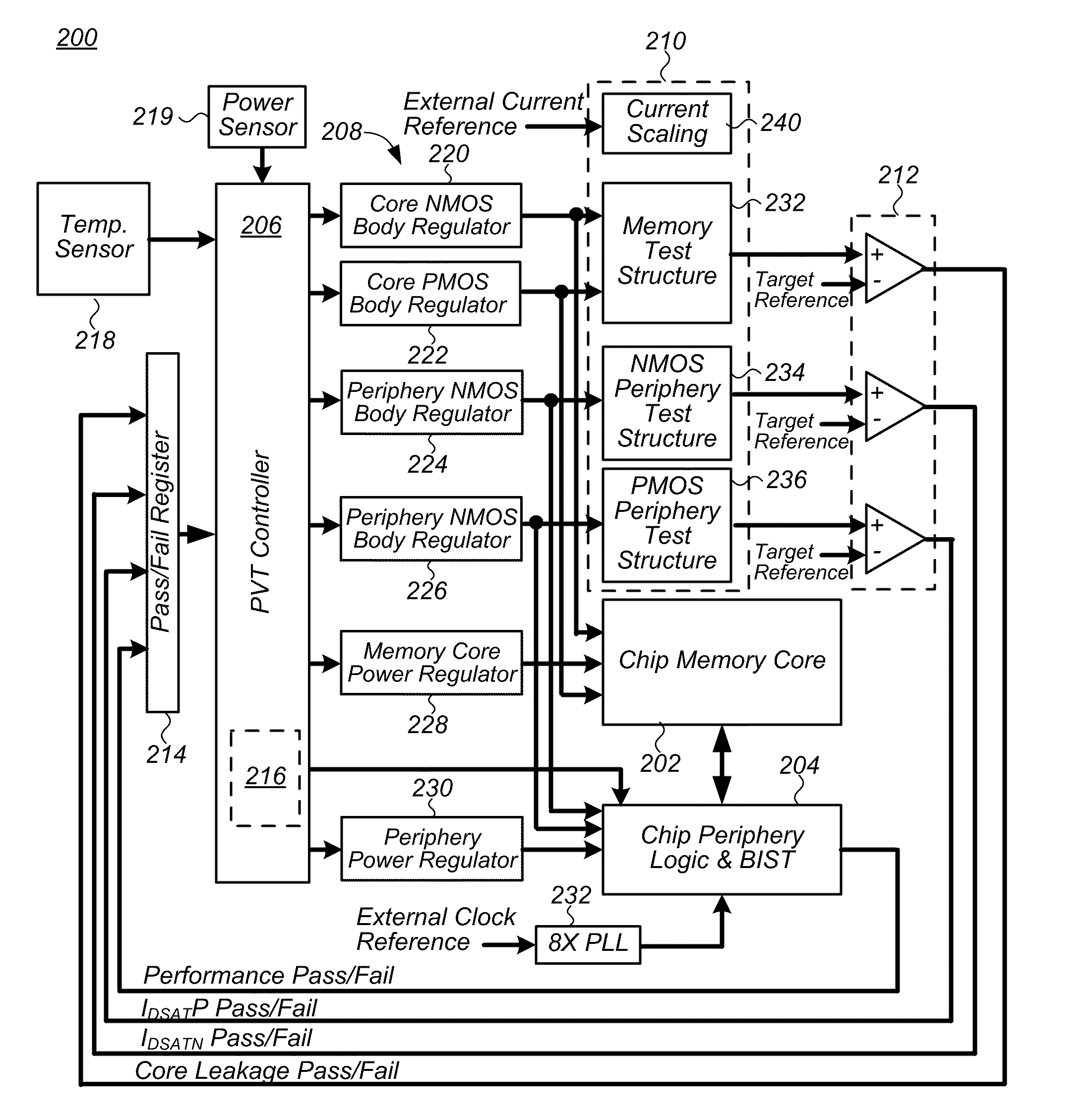
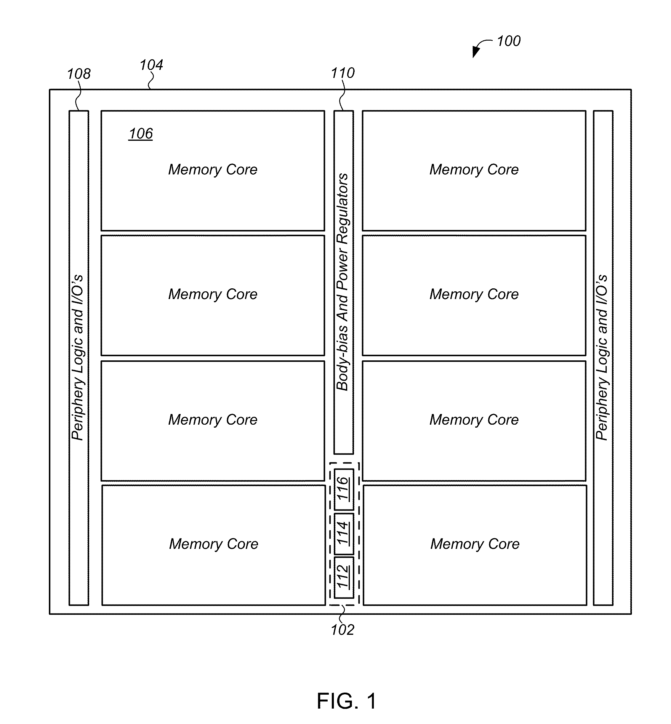
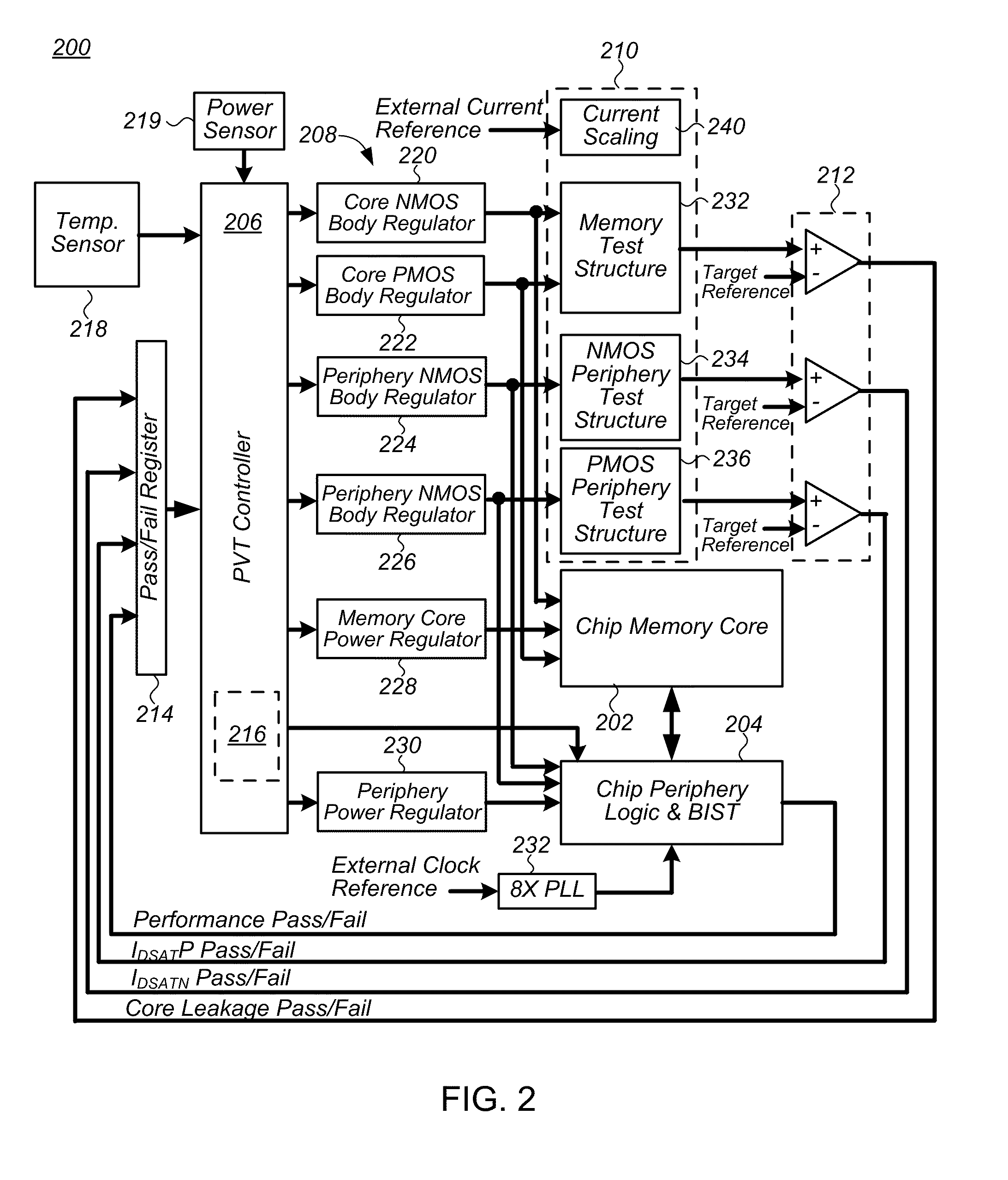
[0020]FIG. 1 is a simplified block diagram in top or plan view of an embodiment of an integrated circuit (IC) 100 including a process, voltage and temperature (PVT) control system 102 that is integrally formed on a shared die 104. The PVT control system 102 performs at least two functions. First, the PVT control system 102 is utilized to calibrate or adjust operating characteristics a number of devices and / or sub-circuits i...


PUM


Abstract

An integrated circuit (IC) including a controller integrally formed on a shared die with the IC and method of operating the same to compensate for process and environmental variations in the IC are provided. In one embodiment the IC is comprised of device and sub-circuits, and the method includes: receiving in the IC electrical power and information on at least one of one or more operational parameters of the IC; and adjusting one or more operating characteristics of at least one of the devices and sub-circuits in the IC based on the received information using a controller integrally formed on a shared die with the IC. Other embodiments are also disclosed.

Description

CROSS-REFERENCE TO RELATED APPLICATIONS[0001]The present application claims the benefit of priority under 35 U.S.C. 119(e) to U.S. Provisional Patent Application Ser. No. 61 / 241,742 entitled “A Microcontroller Based PVT control system For A 65 nm 72 Mb Synchronous SRAM,” filed Sep. 11, 2009, which application is hereby incorporated by reference in its entirety.TECHNICAL FIELD[0002]The present disclosure relates generally to semiconductor devices and more particularly to a system and method to compensating for process and environmental variations in an integrated circuit.BACKGROUND[0003]As scaling of integrated circuit technology continues more challenges emerge in dealing with process and environmental variations. Such variations directly affect operating margin, subthreshold leakage and speed in silicon complimentary-metal-oxide-semiconductor (CMOS) circuits including memory cores and periphery logic devices. Previous schemes or techniques attempting to address such operating margi...

Claims


Application Information

Patent Timeline
IPC IPC(8): G11C5/14H03H11/00H03K3/42
CPCG11C5/143G11C2029/0409G11C29/028G11C5/147
Inventor EID, SHERIFWHATELY, MORGAN ANDREWKRISHNEGOWDA, SANDEEP
Owner INFINEON TECH LLC
Why Eureka
Try Eureka