Embedded SRAM Memory for Low Power Applications

a low-power, embedded technology, applied in the direction of digital storage, instruments, semiconductor devices, etc., can solve the problems of reducing the power, and especially the standby power, of the sram array, and the relatively slow access time of the dram circuit for reads and writes

Active Publication Date: 2011-03-24
TAIWAN SEMICON MFG CO LTD
View PDF7 Cites 15 Cited by
  • Summary
  • Abstract
  • Description
  • Claims
  • Application Information

AI Technical Summary

Benefits of technology

[0026]These and other problems are generally solved or circumvented, and technical advantages are generally achieved by embodiments of the present invention, which provides in a first exemplary embodiment a single core integrated circuit with embedded SRAM bit cells having multiple design rules, to provide different transistor characteristics within one SRAM array, or different transistor characteristics within the embedded SRAMs in a single core with multiple SRAM arrays. The use of different NMOS lightly doped drain (LDD) and pocket implant masks for different portions of the integrated circuit allows some SRAM bit cells to be implemented using the logic design rule transistor characteristics, while other SRAM bit cells are implemented using SRAM device design rules to achieve different characteristics.
[0027]In another embodiment, a dual core integrated circuit, with each core having at least one embedded SRAM array, is provided. In this exemplary embodiment, one core of the dual core integrated circuit may be formed using a first gate dielectric, while the second core may be formed using a second gate dielectric. Further, the use of multiple NMOS LDD implant and pocket implant masks enables the formation of SRAM bit cells that are formed using logic design rules, and SRAM design rules, in each of the two cores. By varying these approaches a range of embodiments is available to allow for low standby power, reduced leakage current, and stable embedded SRAM arrays. The use of different implant steps allows the threshold voltage Vt of the transistors to be controlled. Strong Vt devices may be used in some portions and weaker Vt devices may be used in other portions of the SRAM bit cells.
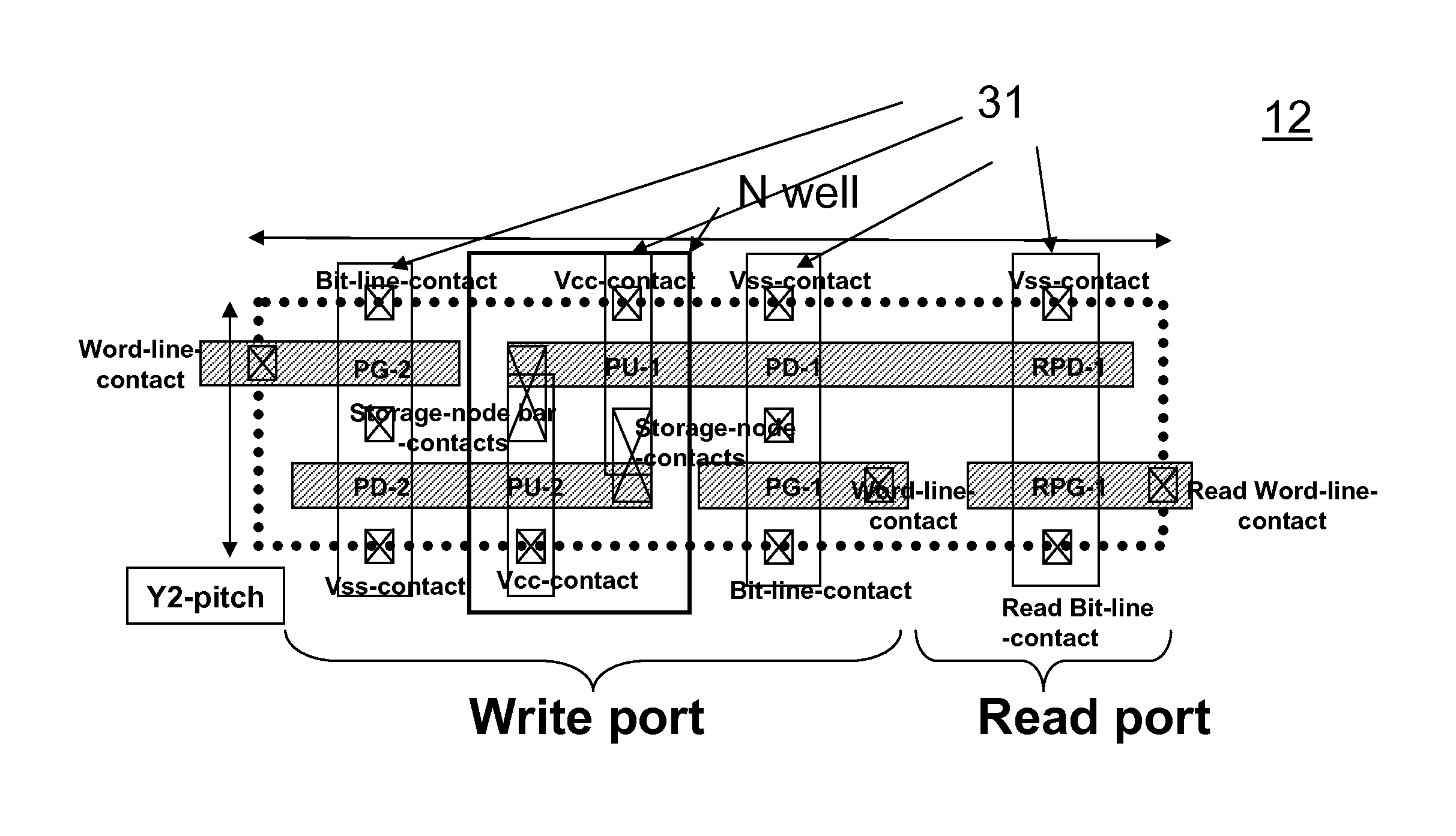
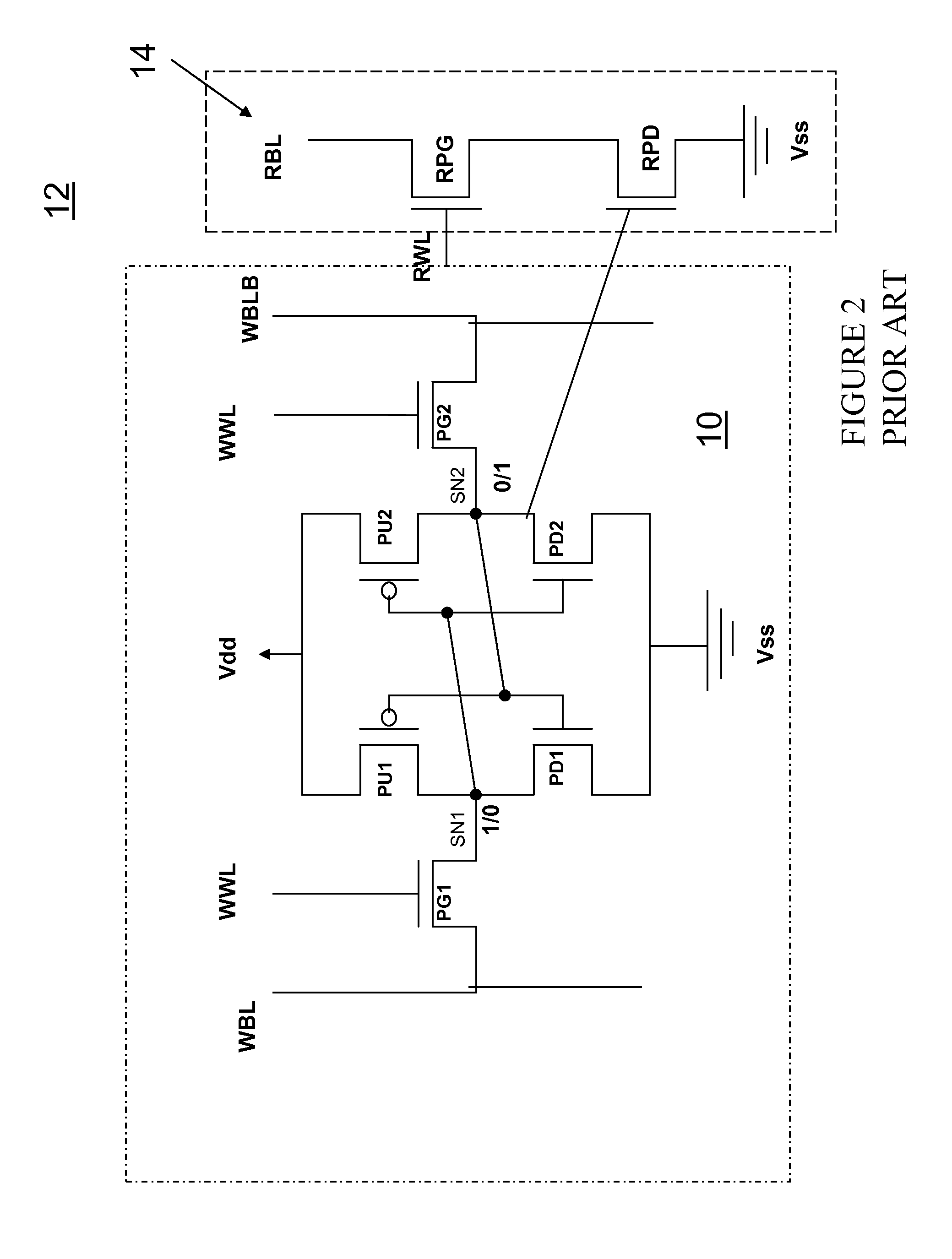
[0029]Further embodiments include a dual core integrated circuit that has embedded SRAM arrays that are both single port and dual port SRAM arrays. The single port SRAM arrays may be formed using thicker gate dielectrics for improved standby leakage current. The dual port SRAM arrays may be formed using the thicker gate dielectrics in the storage bit cell portion, while the read portion transistors are fabricated using the thinner gate dielectrics of the logic portions. In addition, several different NMOS LDD and implant masks may be used to further tailor the transistors in each portion for optimal performance by varying the Vt of the devices.

Problems solved by technology

DRAM cells may be provided in very dense arrays, since a DRAM cell requires only a single access transistor and a storage capacitor, however DRAM circuits have relatively slow access time for reads and writes, and require somewhat complicated control circuitry, and each DRAM cell stores data as charge on a leaky capacitor, so that the DRAM array must be refreshed periodically to maintain state.
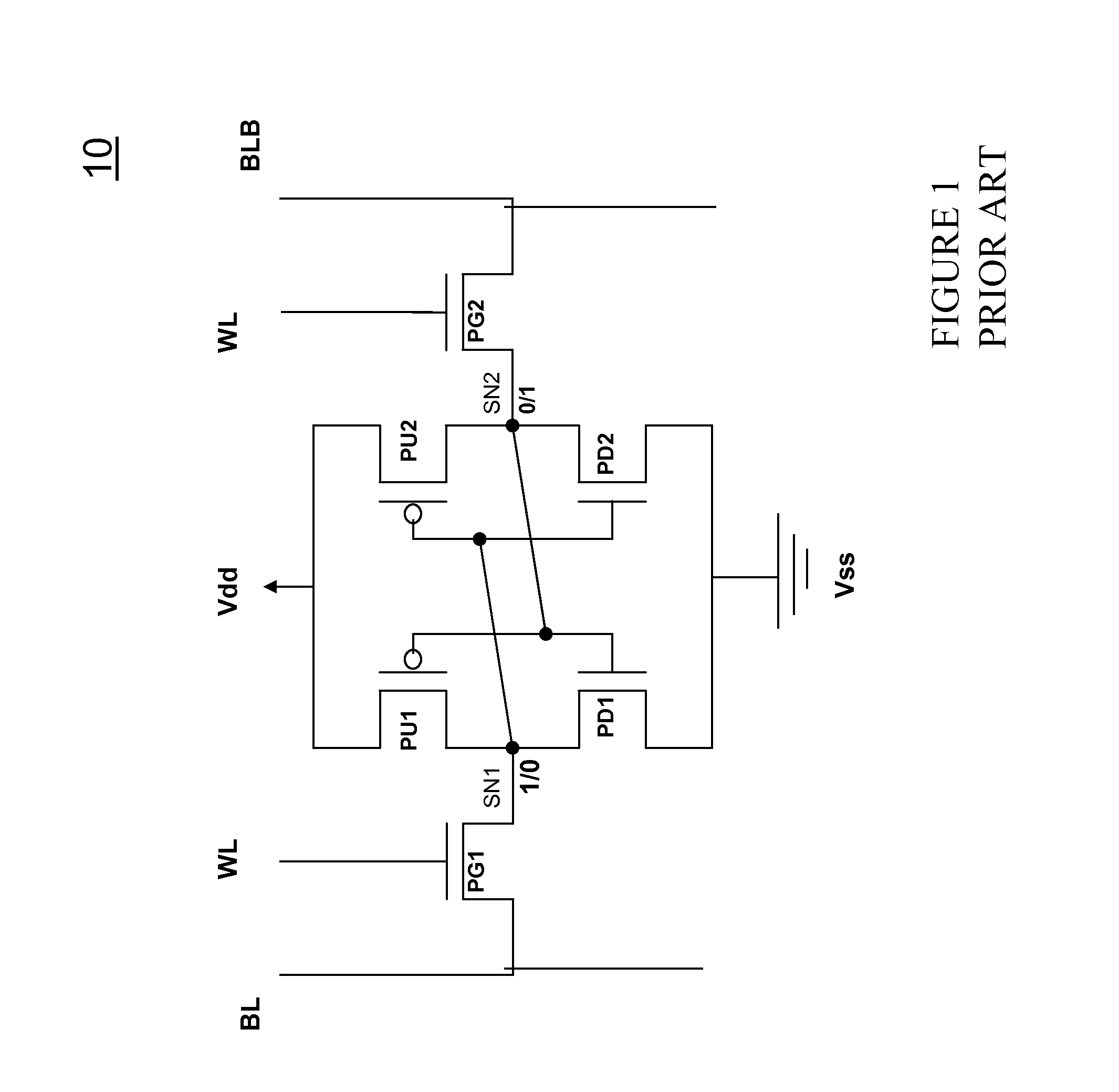
The need to lower the power, and especially the standby power, of the SRAM arrays has also become an issue.
As semiconductor processes advance and device sizes continue to shrink, the ability to reduce power consumption has reached critical limitations.
The SRAM array needs to be stable and retain data, however the usual approach of continuously lowering the supply power to reduce power (Vcc,min) is not compatible with the goals of stability and reducing standby leakage current Isb.
This is difficult to do reliably for the 6T storage cells, however, due to process variations and other constraints increasingly imposed by shrinking device sizes.

Method used


Image

  • Embedded SRAM Memory for Low Power Applications
  • Embedded SRAM Memory for Low Power Applications
  • Embedded SRAM Memory for Low Power Applications

Examples


Embodiment Construction

[0049]The making and using of the presently preferred embodiments are discussed in detail below. It should be appreciated, however, that the present invention provides many applicable inventive concepts that can be embodied in a wide variety of specific contexts. The specific embodiments discussed are merely illustrative of specific ways to make and use the invention, and do not limit the scope of the invention.

[0050]FIG. 8 illustrates in one exemplary embodiment a block diagram where a single core integrated circuit 81 is provided using both logic transistor design rules and SRAM transistor design rules in embedded SRAM arrays in the same core. In FIG. 8, the I / O devices are formed with a first set of design rules for gate dielectric thickness, and a logic portion 45 is again provided with a second set of “Device-1” design rules using a gate oxide dielectric (which may include, for example, oxides, nitrides, oxynitrides, silicon dioxide, and the like as dielectric materials) of a f...


PUM


Abstract

Circuits and methods for providing a dual gate oxide (DGO) embedded SRAM with additional logic portions, where the logic and the embedded SRAM have NMOS transistors having a common gate dielectric thickness but have different lightly doped drain (LDD) implantations formed using different LDD masks to provide optimum transistor operation. In an embodiment, a first embedded SRAM is a single port device and a second embedded SRAM is a dual port device having a separate read port. In certain embodiments, the second SRAM includes NMOS transistors having LDD implants formed using the logic portion LDD mask. Transistors formed with the logic portion LDD mask are faster and have lower Vt than transistors formed using a SRAM LDD mask. Dual core devices having multiple embedded SRAM arrays are disclosed. Methods for making the embedded SRAM are also disclosed.

Description

[0001]This application claims the benefit of U.S. Provisional Application No. 61 / 243,896, entitled “Embedded SRAM Memory for Low Power Applications,” filed on Sep. 18, 2009, which is incorporated herein by reference.CROSS REFERENCE TO RELATED APPLICATION[0002]This application relates to co-pending and co-owned U.S. patent application Ser. No. 12 / 748,098 entitled “Methods and Apparatus for SRAM Bit Cell With Low Standby Current, Low Supply Voltage and High Speed”, Mar. 26, 2010, which claims the benefit of U.S. Provisional Patent Application Ser. No. 61 / 243,941, filed Sep. 18, 2009, both of which are hereby incorporated by reference in their entirety herein.TECHNICAL FIELD[0003]The present invention relates to SRAM memory bit cell structures embedded in an integrated circuit device and having low power requirements. The invention is directed to integrated circuits having SRAM arrays with multiple memory cell types embedded in one integrated circuit along with logic, processors, or ot...

Claims


Application Information

Patent Timeline
Patent Type & Authority Applications(United States)
IPC IPC(8): H01L27/088H01L21/8239
CPCG11C11/412H01L27/1104H01L27/11H10B10/00H10B10/12
Inventor LIAW, JHON-JHY
Owner TAIWAN SEMICON MFG CO LTD
Why Eureka
Try Eureka