Manufacturing method of capacitor in semiconductor device

a manufacturing method and semiconductor technology, applied in the direction of semiconductor devices, electrical devices, transistors, etc., can solve the problems of increasing the cell area of the chip dimension and leakage current, difficult to define the contact hole pattern of the hole type on the mask, and increasing the contact resistan

Active Publication Date: 2011-03-24
SK HYNIX INC
View PDF2 Cites 27 Cited by
  • Summary
  • Abstract
  • Description
  • Claims
  • Application Information

AI Technical Summary

Benefits of technology

[0008]The inventive concept provides an improved contact hole formation method being capable of f

Problems solved by technology

However, it increases a cell area of the chip dimension and a leakage current as compared with a conventional trench type isolation layer.
Accordingly, it is difficult to define the contact hole pattern of a hole type on the mask an

Method used


Image

  • Manufacturing method of capacitor in semiconductor device
  • Manufacturing method of capacitor in semiconductor device
  • Manufacturing method of capacitor in semiconductor device

Examples


Embodiment Construction

”.

BRIEF DESCRIPTION OF THE DRAWINGS

[0019]The above and other aspects, features and other advantages of the subject matter of the present disclosure will be more clearly understood from the following detailed description taken in conjunction with the accompanying drawings, in which:

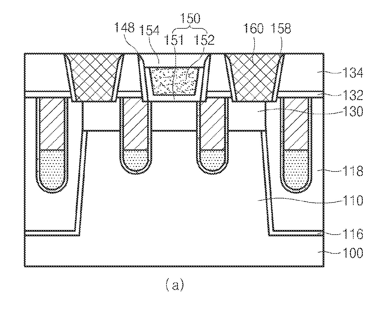
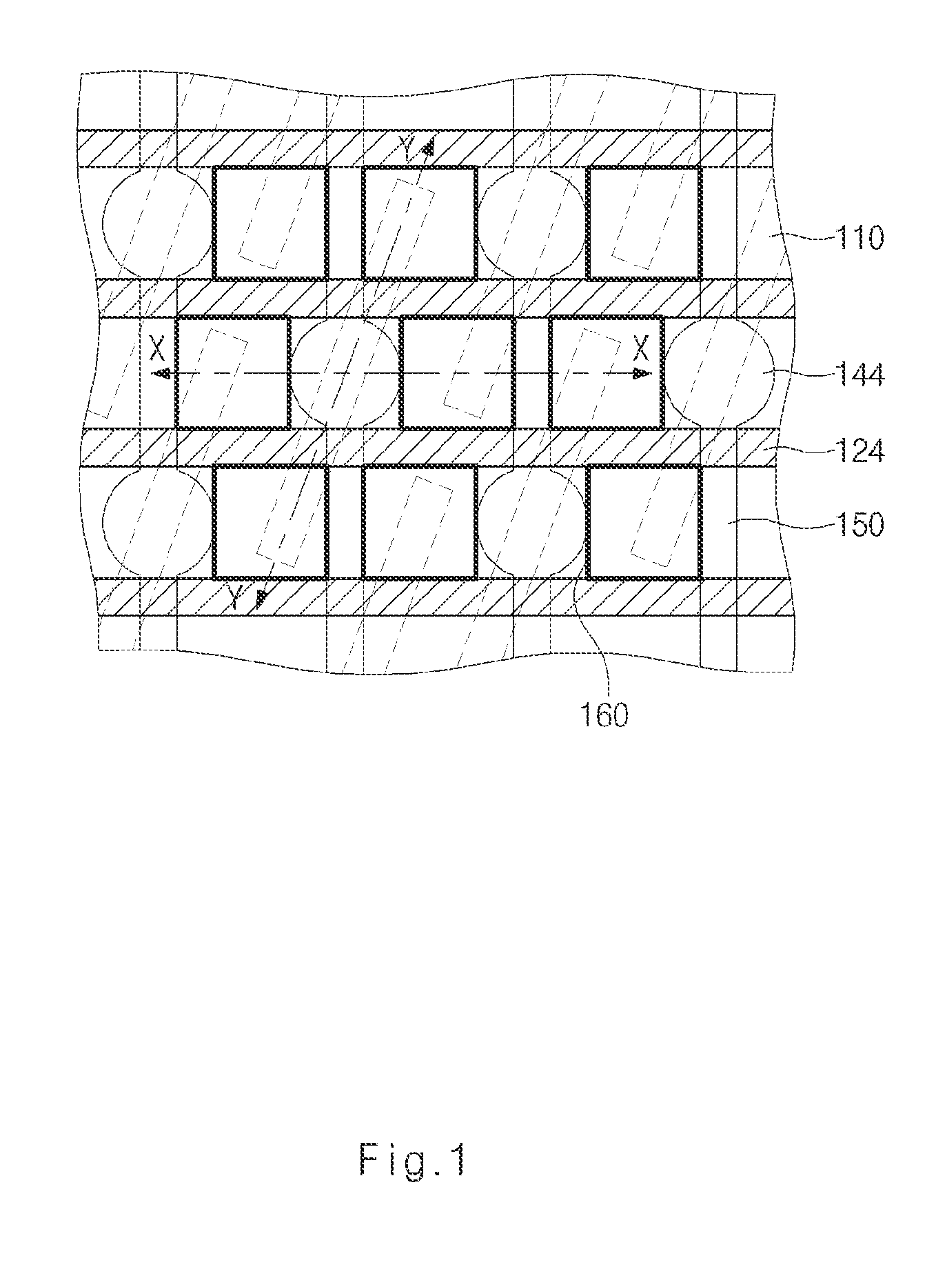
[0020]FIG. 1 a plan view illustrating a layout of a semiconductor device according to an embodiment of the present invention;

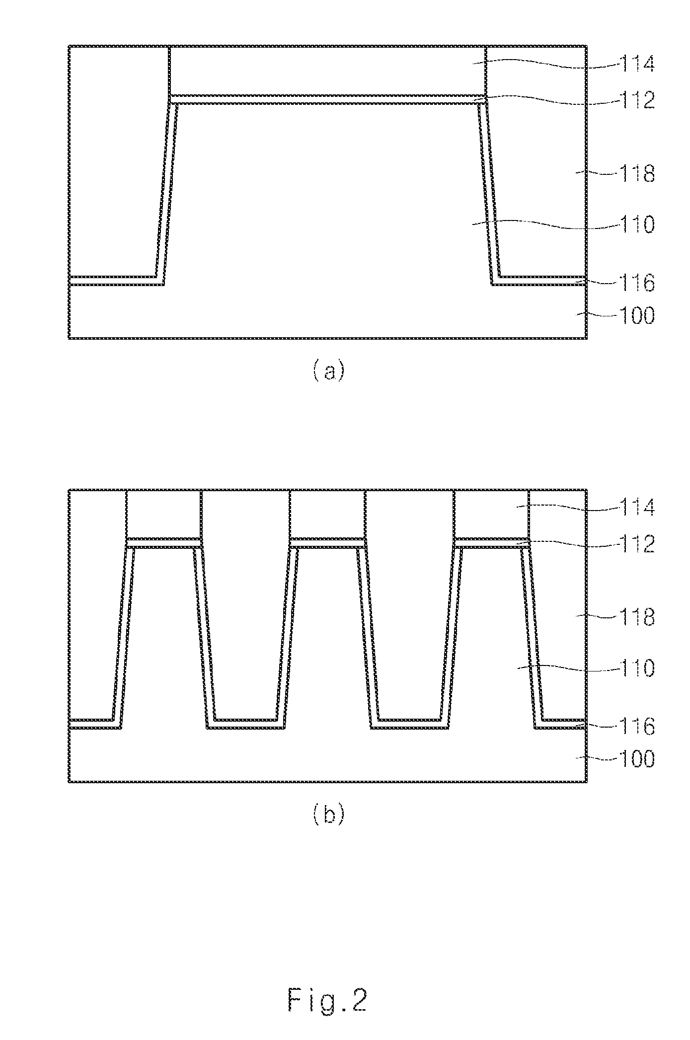
[0021]FIGS. 2a through 12a are sectional views in a Y-axis direction of FIG. 1;

[0022]FIGS. 2b through 12B are sectional views in a X-axis direction of FIG. 1; and

[0023]FIG. 13 is a diagram illustrating a layout of a photo mask according to an embodiment of the present invention.

DESCRIPTION OF EMBODIMENTS

[0024]Hereinafter, embodiments of the present invention will now be described more fully with reference to the accompanying drawings. The embodiments may, however, be embodied in many different forms and should not be construed as being limited to the instances set forth herein. Rathe...


PUM


Abstract

Example embodiment is provided to a method for manufacturing a semiconductor device, including forming a hard mask layer on a buried bit line and forming a storage node contact hole by using the selectivity between an interlayer insulating layer and the hard mask layer, thereby forming a contact hole using a mask of a line pattern instead of a hole pattern. Accordingly, a mask for the contact hole can be easily fabricated and the contact area can be maximized, thereby reducing the contact resistance.

Description

CROSS-REFERENCES TO RELATED APPLICATION[0001]Priority to Korean patent application number 10-2009-0088371, filed on Sep. 18, 2009, which is incorporated by reference in its entirety, is claimed.BACKGROUND OF THE INVENTION[0002]The embodiments described herein relate to a method for manufacturing a semiconductor device and, more particularly, to a method for manufacturing a semiconductor device being capable of easily forming a hole type contact hole in a highly integrated semiconductor device and maximizing an open area of an active region.[0003]So as to increase integration of the semiconductor device, various methods that integrate more circuit patterns in the limited area by modifying cell layout have been suggested. One of the methods is to modify an arrangement of the active regions which transistors are embedded therein from an 8F2 cell layout to a 6F2 cell layout.[0004]In a DRAM, word lines are arranged to be orthogonally crossed to bit lines and active regions are repeatedly...

Claims


Application Information

Patent Timeline
IPC IPC(8): H01L21/02
CPCH01L21/76897H01L27/10876H01L27/10855H01L27/10814H10B12/315H10B12/053H10B12/0335H10B99/00H10B12/00
Inventor KIM, JI HYE
Owner SK HYNIX INC
Why Eureka
Try Eureka