
Signal Acquisition System Having Reduced Probe Loading of a Device Under Test

a signal acquisition and probe technology, applied in the field of signal acquisition systems, can solve the problems of increasing the divider ratio of the network, the shunting of resistive center conductor signal cables to ground, and the substantial portion of the mid-band and high-band frequency signal current, so as to maintain the flatness over the frequency bandwidth of the signal acquisition system

Active Publication Date: 2011-03-31
TEKTRONIX INC
View PDF28 Cites 20 Cited by
  • Summary
  • Abstract
  • Description
  • Claims
  • Application Information

AI Technical Summary

Benefits of technology

[0011]Accordingly, the present invention is a signal acquisition system having a signal acquisition probe and a signal processing instrument. The signal acquisition probe has probe tip circuitry coupled to a resistive center conductor signal cable. The resistive center conductor signal cable is coupled to an input node of the signal processing instrument. The input node is further coupled to a compensation system dispos

Problems solved by technology

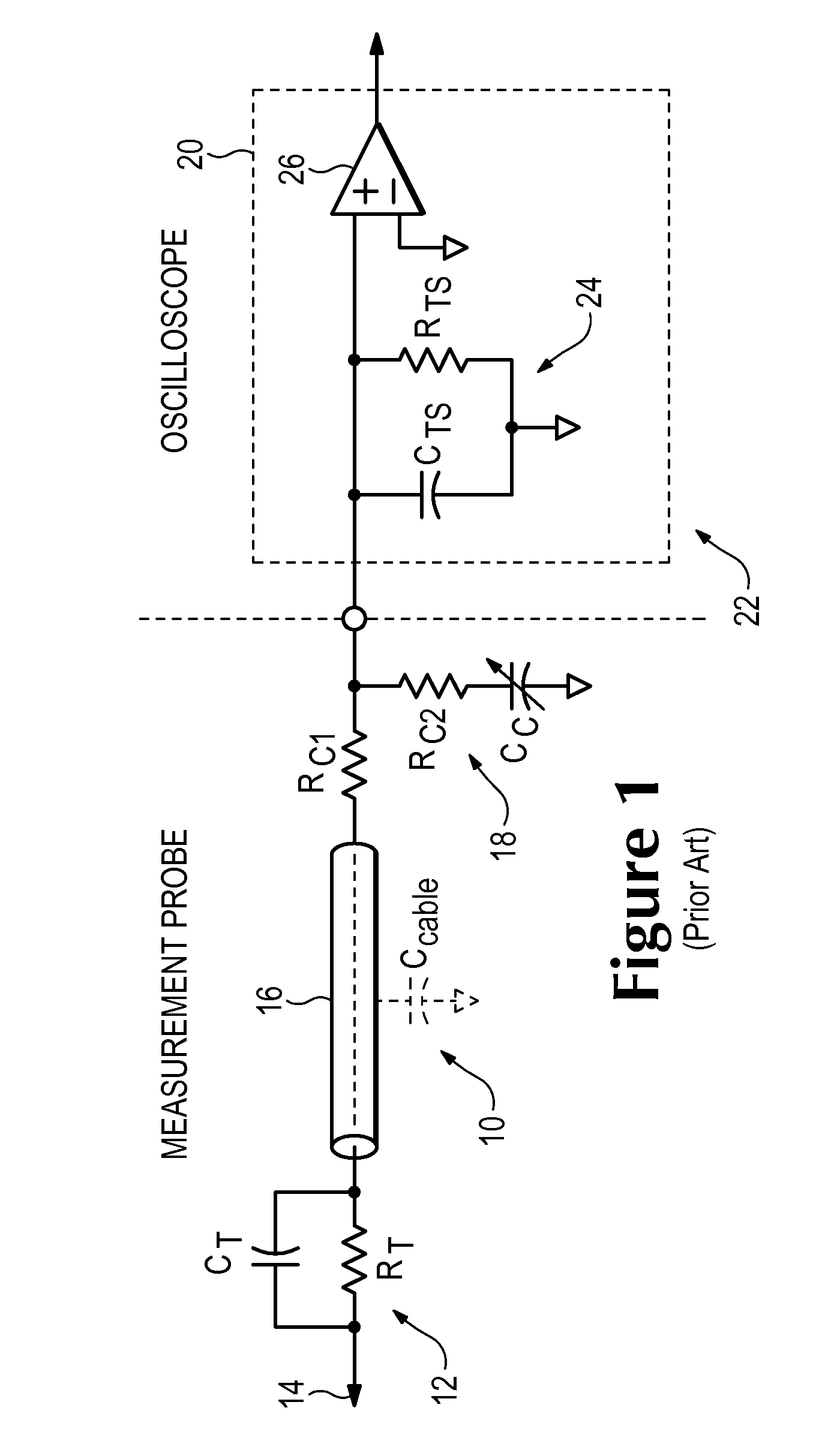
A major drawback to existing passive voltage probe and oscilloscope configurations is that a substantial portion of the mid-band and high-band frequency signal current at the output of the resistive center conductor signal cable is shunted to ground by the termination capacitor CC.
However, this increases the divider ratio of the network with a resulting increase in the attenuation of signal applied to the probe.
The decreased signal input to the oscilloscope may be compensated for by increasing the gain of the oscilloscope input circuits which results in an increase in the noise on the signal reducing the overall signal-to-noise ratio of the instrument.
The voltage input to this probe is limited as compared to the traditional passive probe due to the size of the input resistor.
Also, the low input resistance can cause excessive loading to DC signals.

Method used


Image

  • Signal Acquisition System Having Reduced Probe Loading of a Device Under Test
  • Signal Acquisition System Having Reduced Probe Loading of a Device Under Test
  • Signal Acquisition System Having Reduced Probe Loading of a Device Under Test

Examples


Embodiment Construction

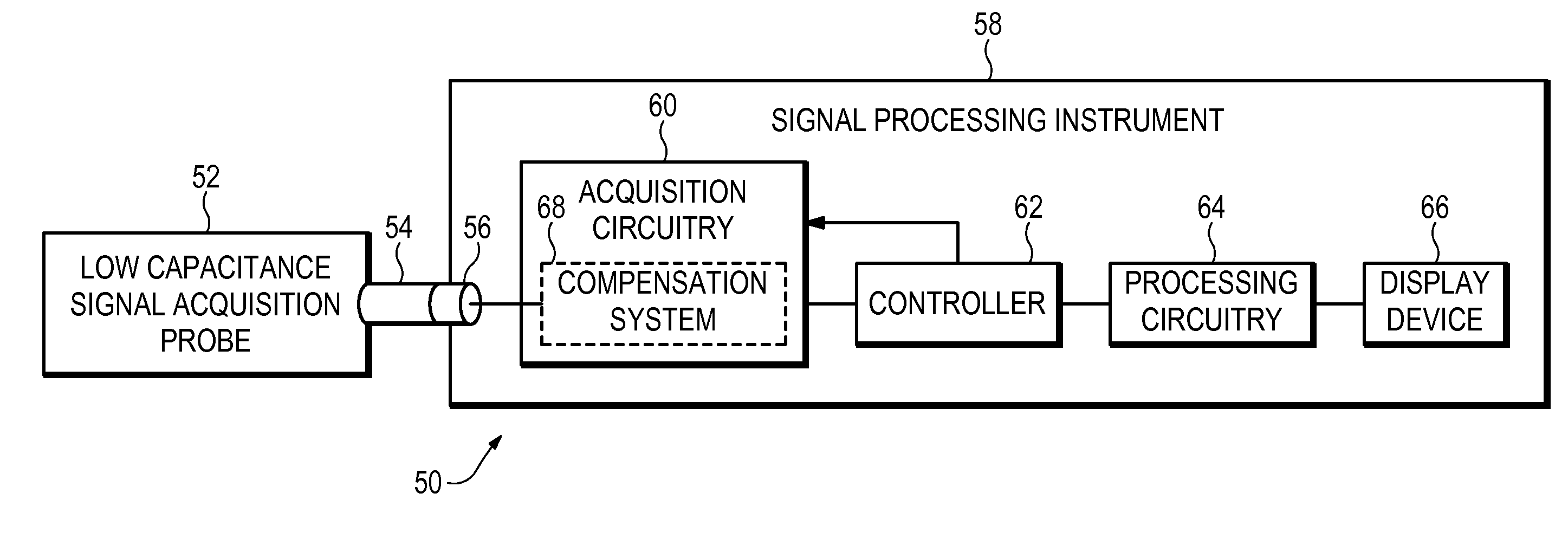
[0029]Referring to FIG. 4, there is shown a high level block diagram of a signal acquisition system 50 having reduced probe loading of a device under test according to the present invention. The signal acquisition system 50 has a signal acquisition probe 52 that includes a resistive center conductor signal cable 54. The signal cable is coupled to an input node 56 of a signal processing instrument 58. The input node 56 is also coupled to acquisition circuitry 60 in the signal processing instrument 58. The acquisition circuitry 60 generates digital values of an input signal from the signal acquisition probe 52. The digital values of the input signal are coupled to a controller 62 for further processing. The controller 62 may couple the digital values to processing circuitry 64 for formatting the digital values and displaying the formatted digital values on a display device 66.

[0030]In traditional probe-oscilloscope system, each stage of the signal path is compensated for a flat freque...


PUM


Abstract

A signal acquisition system has a signal acquisition probe having probe tip circuitry coupled to a resistive center conductor signal cable. The resistive center conductor signal cable of the signal acquisition probe is coupled to a compensation system in a signal processing instrument via an input node and input circuitry in the signal processing instrument. The signal acquisition probe and the signal processing instrument have mismatched time constants at the input node with the compensation system having an input amplifier with feedback loop circuitry and a shunt pole-zero pair coupled to the input circuitry providing pole-zero pairs for maintaining flatness over the signal acquisition system frequency bandwidth.

Description

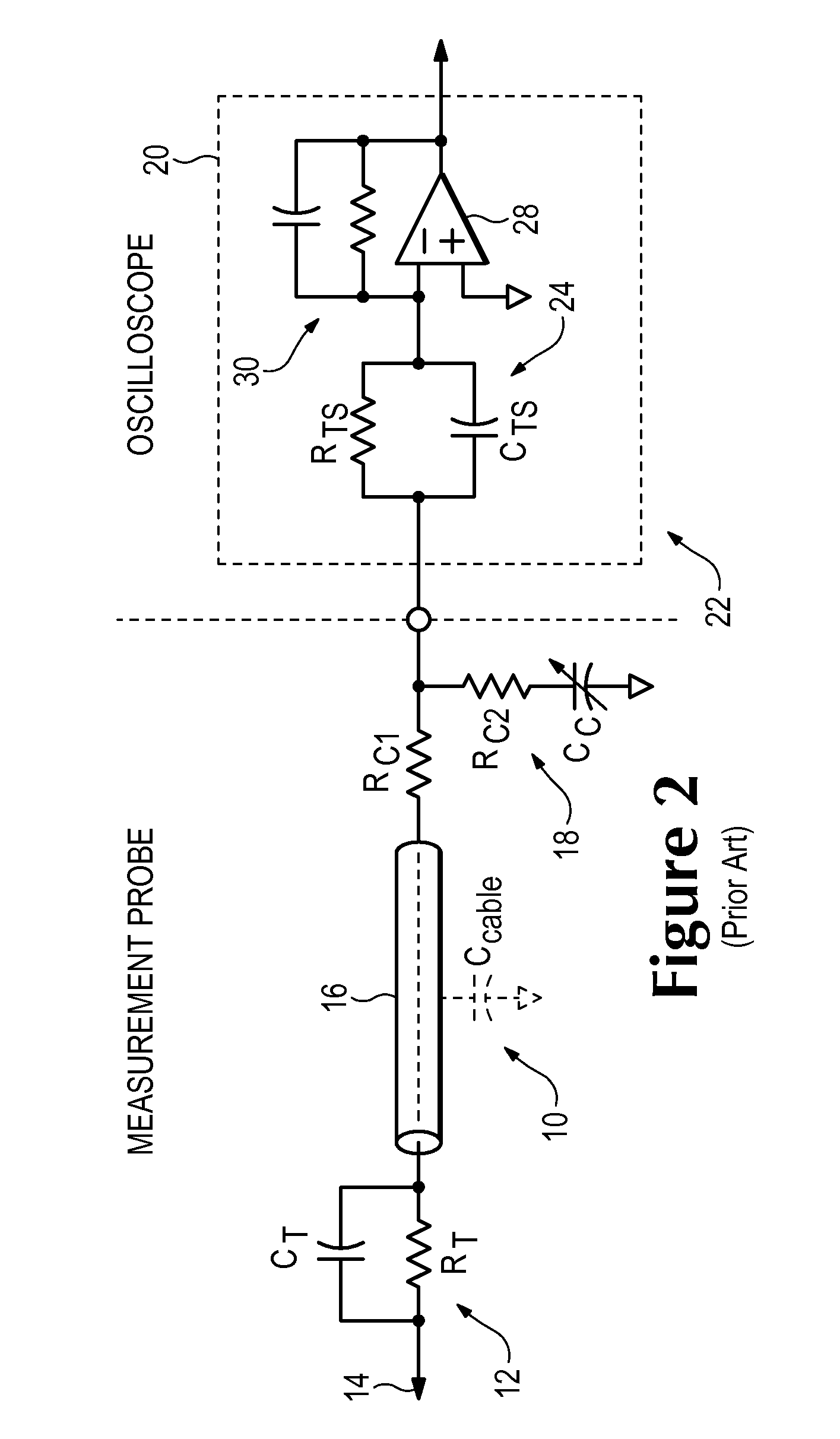
CROSS REFERENCE TO RELATED APPLICATION[0001]This Continuation-in-Part application claims priority from U.S. patent application Ser. No. 12 / 571,236, filed Sep. 30, 2009.BACKGROUND OF THE INVENTION[0002]The present invention relates generally to acquiring a signal from a device under test and more particularly to a signal acquisition system having reduced loading of the device under test using a signal acquisition probe with reduced capacitance.[0003]Traditional passive voltage probes 10 generally consist of a resistive-capacitive parallel network 12 at the probe tip 14, shown as RT and CT in FIG. 1, coupled via a resistive center conductor signal cable 16 to compensation circuitry 18 in a compensation box. The compensation circuitry 18 has resistive elements RC1 and RC2 and capacitive element CC. RC1 is in series with the cable 16 and RC2 is in series with variable capacitor CC. The compensation circuitry 18 is coupled to input circuitry 20 of a measurement test instrument 22, such a...

Claims


Application Information

Patent Timeline
IPC IPC(8): G01R23/165
CPCG01R1/06766G01R23/16G01R1/06772G01R35/00
Inventor BARTLETT, JOSIAH A.POLLOCK, IRA G.KNIERIM, DANIEL G.LARSON, LESTER L.JANSEN, SCOTT R.DOBYNS, KENNETH P.STEVENS, MICHAEL DUANE
Owner TEKTRONIX INC
Learn More