

Thermoelectric conversion device
a conversion device and thermal conductivity technology, applied in the field of thermal conductivity conversion devices, can solve the problems of insufficient efficiency of current seebeck effect elements, and achieve the effects of low thermal conductivity, easy to provide a uniform temperature gradient, and high efficiency
- Summary
- Abstract
- Description
- Claims
- Application Information
AI Technical Summary
Benefits of technology
Problems solved by technology
Method used
Image

Examples
first embodiment
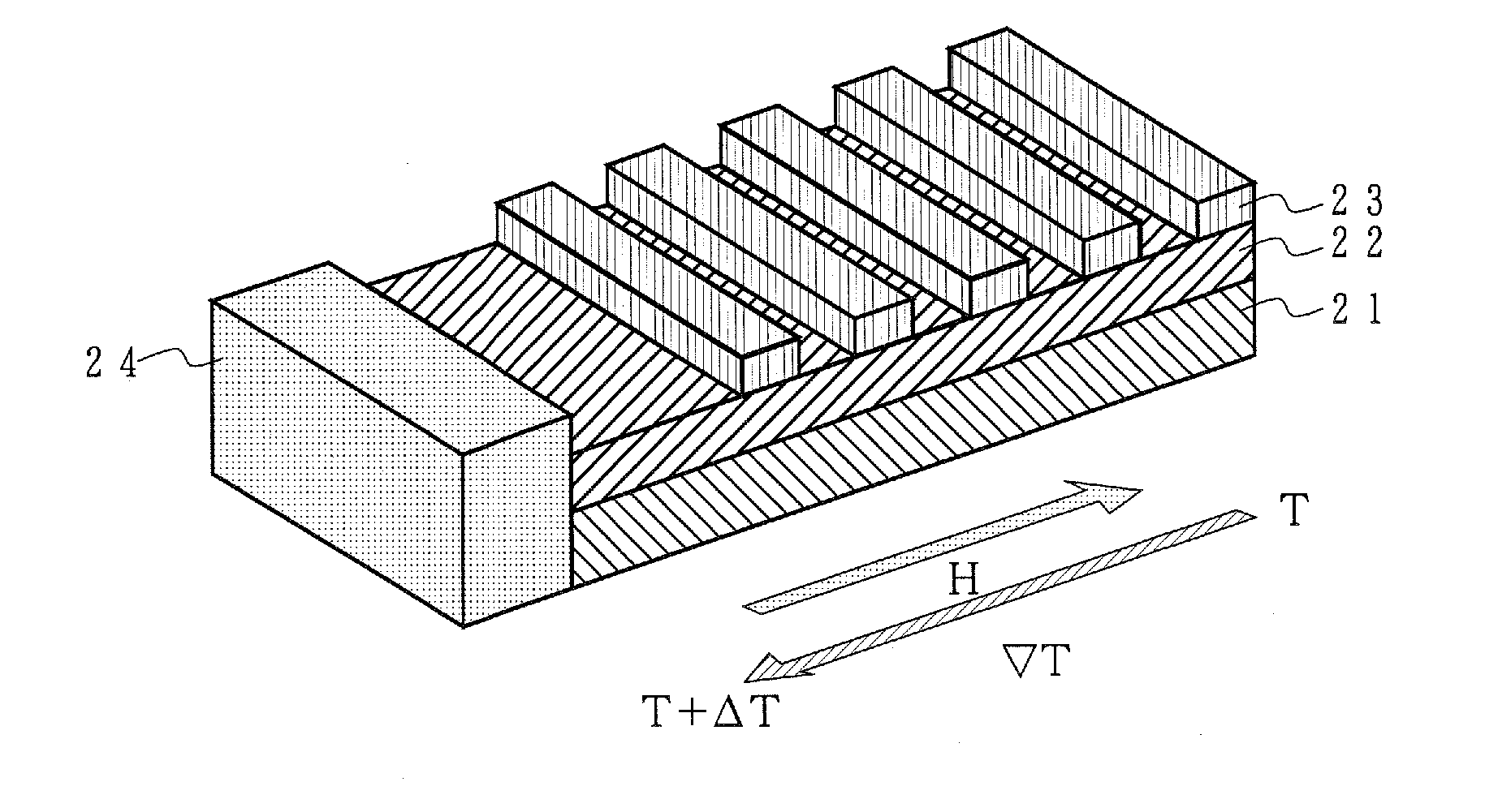
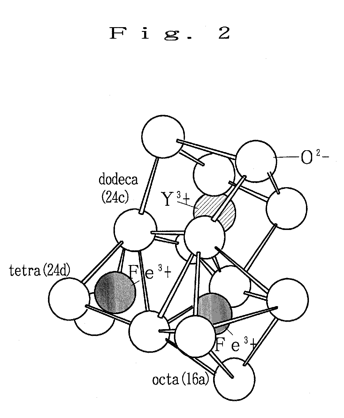
[0065]Next, the thermoelectric conversion device according to the first embodiment of the present invention is described in reference to FIG. 6. FIG. 6 is a schematic perspective diagram showing the thermoelectric conversion device according to the first embodiment of the present invention, where a YIG layer 22 containing Y3Fe4GaO12 having a thickness of 100 nm is formed on a GGG single crystal substrate 21 in accordance with a sputtering method, and a Pt film having a thickness of 10 nm and a width of 0.6 mm is deposited on top in accordance with a mask sputtering method so that a Pt electrode 23 is formed, and thus the thermoelectric conversion device according to the first embodiment of the present invention is provided.
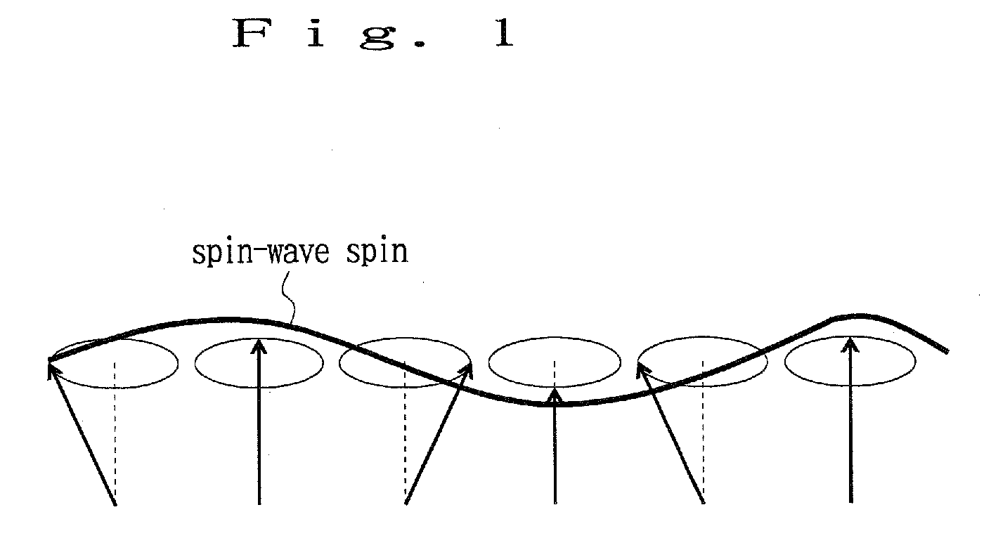
[0066]FIG. 7 is a diagram showing how the thermoelectric conversion device according to the first embodiment of the present invention is used. As shown in FIG. 7, when an external magnetic field H is applied in a direction perpendicular to the longitudinal directi...
second embodiment
[0068]Next, the thermoelectric conversion device according to the second embodiment of the present invention is described in reference to FIG. 8. FIG. 8 is a schematic perspective diagram showing the thermoelectric conversion device according to the second embodiment of the present invention, where a YIG layer 22 containing Y3Fe4GaO12 having a thickness of 100 nm is formed on a GGG single crystal substrate 21 in accordance with a sputtering method, and five Pt films having a thickness of 10 nm and a width of 0.1 mm are deposited on top with intervals of 0.6 mm in accordance with a mask sputtering method so that five Pt electrodes 23 are formed, and thus the thermoelectric conversion device according to the second embodiment of the present invention is provided. FIG. 8 is a schematic diagram, and does not show the actual dimensions of the Pt electrodes 23.
[0069]FIG. 9 is a diagram showing how the thermoelectric conversion device according to the second embodiment of the present inven...
third embodiment
[0071]Next, the thermoelectric conversion device according to the third embodiment of the present invention is described in reference to FIG. 10. FIG. 10 is a schematic perspective diagram showing the thermoelectric conversion device according to the third embodiment of the present invention, where an InMn antiferromagnetic layer 32 having a thickness of 50 nm is deposited on top of a GGG single crystal substrate 31 in accordance with a sputtering method. A YIG layer 33 having a Y3Fe4Ga12 composition and a thickness of 100 nm is formed on top of this. Furthermore, a Pt film having a thickness of 10 nm and a width of 0.1 mm is deposited on top in accordance with a mask sputtering method as a Pt electrode 34, and thus the thermoelectric conversion device according to the third embodiment of the present invention is provided. Here, when the InMn antiferromagnetic layer 32 is deposited, a magnetic field is applied in a direction perpendicular to the longitudinal direction of the Pt elec...
PUM
 Abstract
Description
Claims
Application Information