METHOD OF DEPOSITING DIELECTRIC FILM HAVING Si-N BONDS BY MODIFIED PEALD METHOD
a dielectric film and dielectric film technology, applied in chemical vapor deposition coating, coating, metallic material coating process, etc., can solve the problems of poor conformality or poor step coverage on a substrate containing small features, poor conformal coverage hampering the development of higher density circuit devices and elements, and extremely poor deposition rate. , to achieve the effect of high conformality, high deposition rate and high conformality
- Summary
- Abstract
- Description
- Claims
- Application Information
AI Technical Summary
Benefits of technology
Problems solved by technology
Method used
Image
Examples
example 2
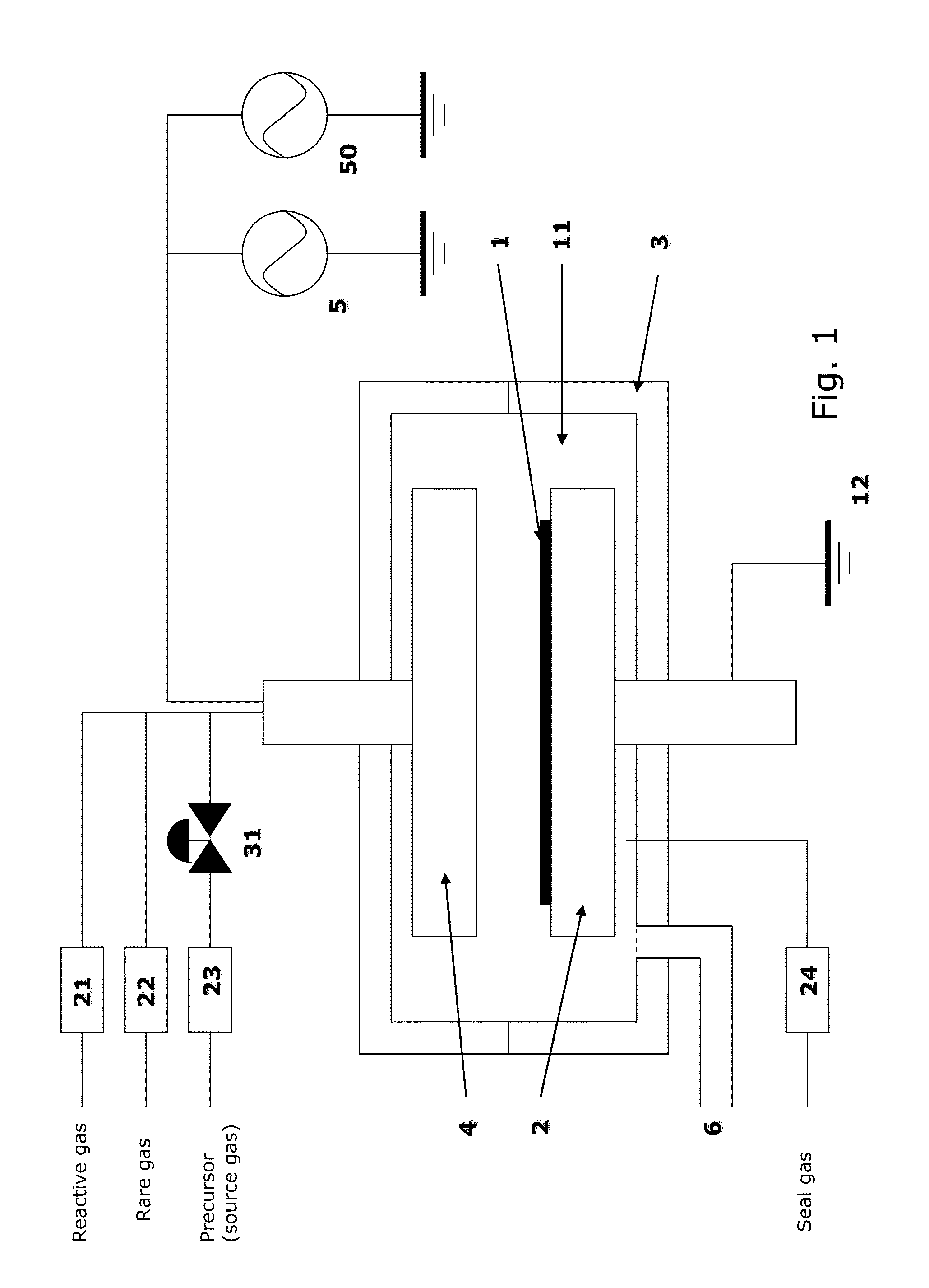
[0110]A dielectric layer having Si—N bonds was formed on a substrate under the condition shown below using the sequence illustrated in FIG. 3 and the PEALD apparatus illustrated in FIG. 1.
[0111]Trisilylamine: 100 sccm
[0112]Hydrogen: 500 sccm
[0113]Nitrogen: 1000 sccm
[0114]Process helium: 1400 sccm
[0115]Sealed helium: 500 sccm
[0116]Argon: 500 sccm
[0117]Substrate temperature: 350° C.
[0118]High frequency RF power (a frequency of 13.56 MHz): 0.07 W / cm2
[0119]Low frequency RF power (a frequency of 430 kHz): 0.0 W / cm2
[0120]Trisilylamine supply time: 1.0, 0.7, 0.5, and 0.1 sec supply
[0121]RF Plasma exciting time: 1.0 sec excite
[0122]Purge time: 1.0 sec interval with reactive gases
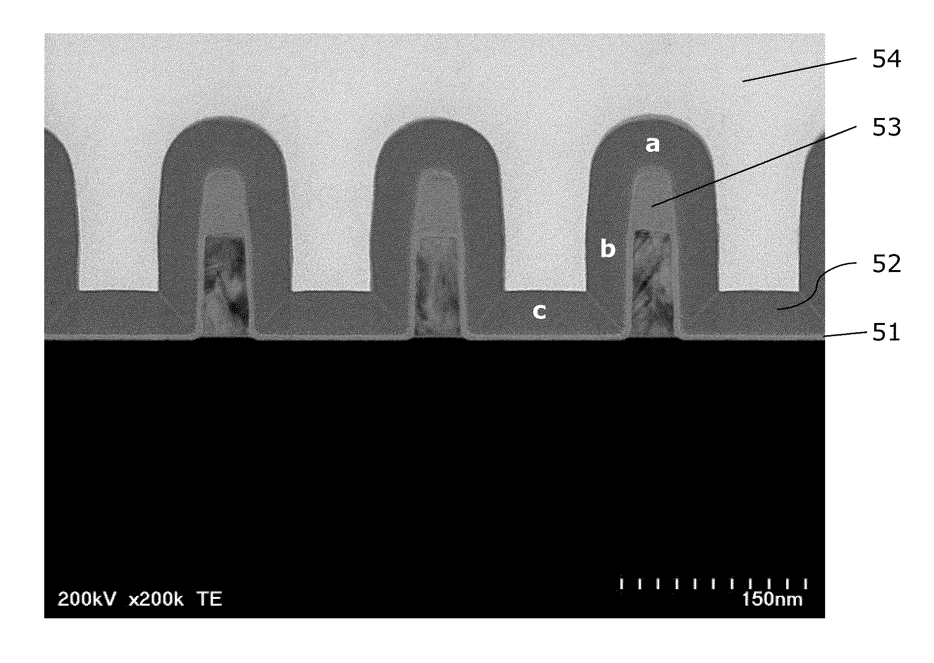
[0123]FIG. 4 shows film thickness per cycle of the comparative PEALD method and the disclosed embodiments of the present invention method. In case of the disclosed embodiments (immediate RF plasma), the film thickness per cycle is approximately 0.17˜0.19 nm / cycle as shown in line “b” (1.0 sec pulse of precursor su...
example 3
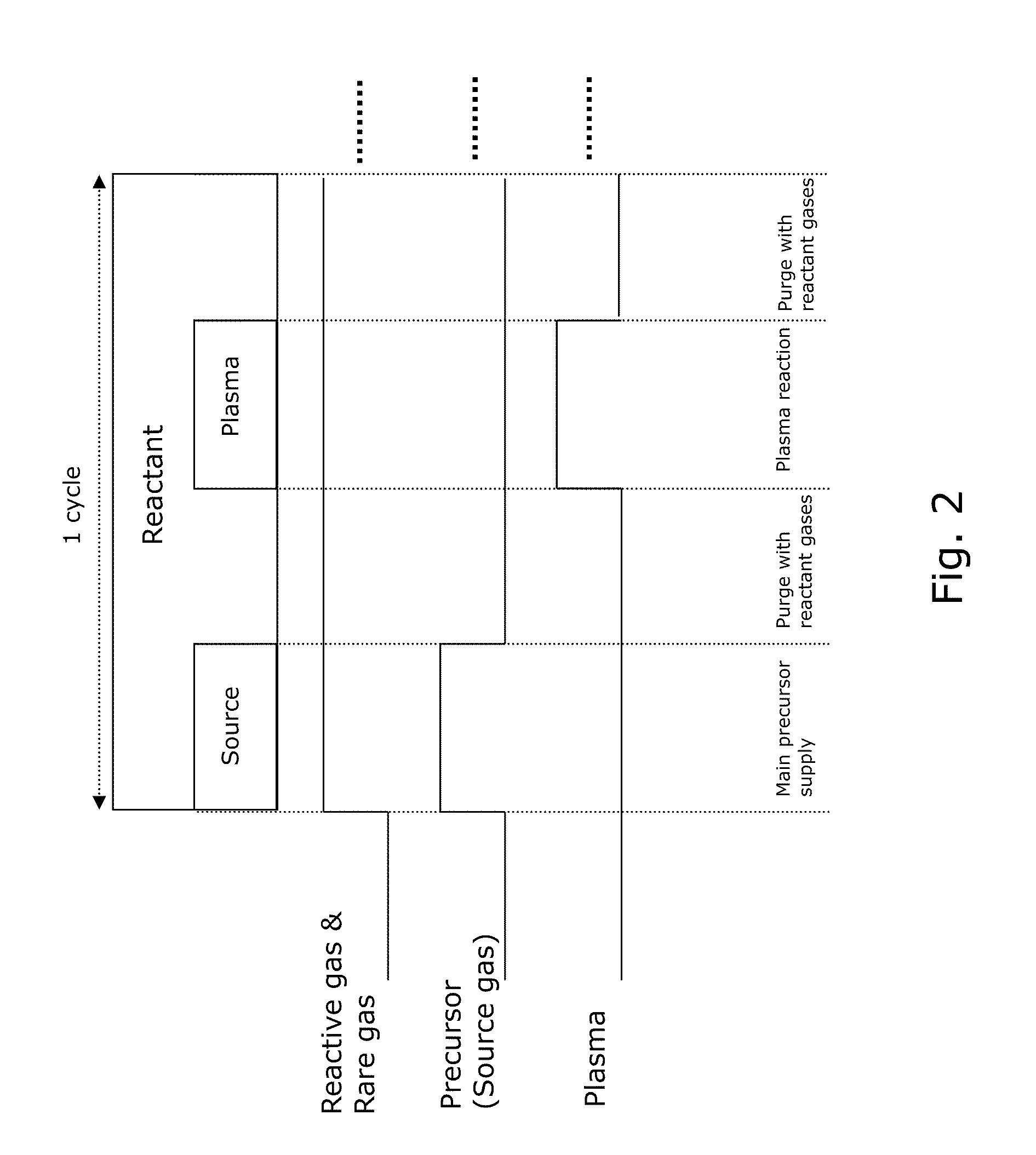
[0127]A dielectric layer having Si—N bonds was formed with second precursor, for example ammonia, on a substrate under the condition shown below using the sequence illustrated in FIG. 2 and the PEALD apparatus illustrated in FIG. 1.
[0128]Trisilylamine: 100 sccm
[0129]Hydrogen: 500 sccm
[0130]Nitrogen: 1000 sccm
[0131]Ammonia: 300 sccm
[0132]Process helium: 1400 sccm
[0133]Sealed helium: 500 sccm
[0134]Argon: 500 sccm
[0135]Substrate temperature: 350° C.
[0136]High frequency RF power (a frequency of 13.56 MHz): 0.07 W / cm2
[0137]Low frequency RF power (a frequency of 430 kHz): 0.0 W / cm2
[0138]Trisilylamine supply time: 1.0 sec supply
[0139]Second precursor (Ammonia) supply time: 1.0 sec supply
[0140]RF Plasma exciting time: 1.0 sec excite
[0141]Purge time: 1.0 sec interval with reactive gases
[0142]In case of adding ammonia, the film thickness per cycle is approximately 0.25 nm / cycle. Deposited dielectric film having Si—N bonds with adding NH3 has wet etch rate 37 nm / min under BHF130 etchant.
example 4
[0143]A dielectric layer having Si—N bonds was formed with second precursor, for example Bis(ethylmethylamino)silane, on a substrate under the condition shown below using the sequence illustrated in FIG. 2 and the PEALD apparatus illustrated in FIG. 1.
[0144]Trisilylamine: 100 sccm
[0145]Hydrogen: 500 sccm
[0146]Nitrogen: 1000 sccm
[0147]Bis(ethylmethylamino)silane: 300 sccm
[0148]Process helium: 1400 sccm
[0149]Sealed helium: 500 sccm
[0150]Argon: 500 sccm
[0151]Substrate temperature: 350° C.
[0152]High frequency RF power (a frequency of 13.56 MHz): 0.07 W / cm2
[0153]Low frequency RF power (a frequency of 430 kHz): 0.0 W / cm2
[0154]Trisilylamine supply time: 1.0 sec supply
[0155]Second precursor (Bis(ethylmethylamino)silane) supply time: 1.0 sec supply
[0156]RF Plasma exciting time: 1.0 sec excite
[0157]Purge time: 1.0 sec interval with reactive gases
[0158]In case of adding Bis(ethylmethylamino)silane, the film thickness per cycle is approximately 0.17 nm / cycle. Deposited dielectric film having ...
PUM
| Property | Measurement | Unit |
|---|---|---|
| Fraction | aaaaa | aaaaa |
| Time | aaaaa | aaaaa |
| Time | aaaaa | aaaaa |
Abstract
Description
Claims
Application Information


