Microfabrication of Carbon-based Devices Such as Gate-Controlled Graphene Devices

a technology of carbon-based devices and gate-controlled graphene, which is applied in the field of carbon-based forms, can solve the problems of the state-of-the-art cnt production technology not being able to reliably make cnt of one type or the other

Inactive Publication Date: 2011-04-21
PRESIDENT & FELLOWS OF HARVARD COLLEGE
View PDF2 Cites 92 Cited by
  • Summary
  • Abstract
  • Description
  • Claims
  • Application Information

AI Technical Summary

Benefits of technology

[0007]The invention provides graphene configurations for producing robust and reproducible gate-controlled graphene devices having an arbitrary n

Problems solved by technology

Exactly two-thirds of all CNT made are semiconducting while the remaining third are metallic, with

Method used


Image

  • Microfabrication of Carbon-based Devices Such as Gate-Controlled Graphene Devices
  • Microfabrication of Carbon-based Devices Such as Gate-Controlled Graphene Devices
  • Microfabrication of Carbon-based Devices Such as Gate-Controlled Graphene Devices

Examples


example i

[0077]A semiconducting carbon nanotube was synthesized. and was configured for initial conductance characterization in a pristine state. A source-drain dc transport measurement was made by contacting ends of the nanotube. FIG. 8A is a plot of differential conductance, g, as a function of backgate voltage, V, for the pristine nanotube.

[0078]The carbon nanotube was then processed to form a functionalization layer and an oxide layer on the full circumference and length of the cylindrical sidewall of the nanotube. The nanotube was inserted into an ALD reaction chamber and the chamber was pumped down to a pressure of 0.3 torr. 5 ALD cycles were then conducted at room temperature to form a functionalization layer by the following process. A 100 torr dose of NO2 gas was first introduced into the chamber for 0.5 seconds and then pumped out. Following a 10 second purge under continuous flow of 20 sccm of N2, a 1 torr dose of tetrakis(dimethylamido)hafnium(IV) (TDH) vapor was pulsed into the ...

example ii

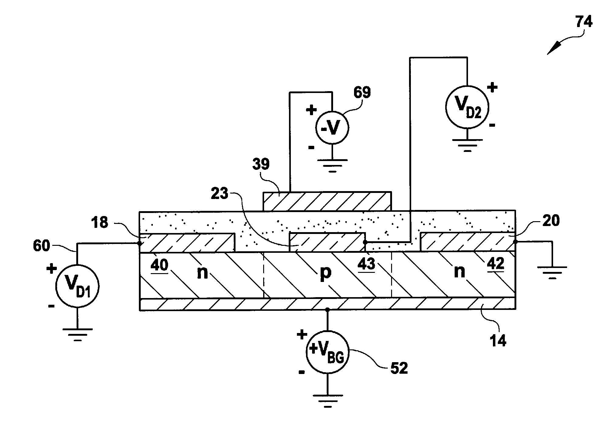
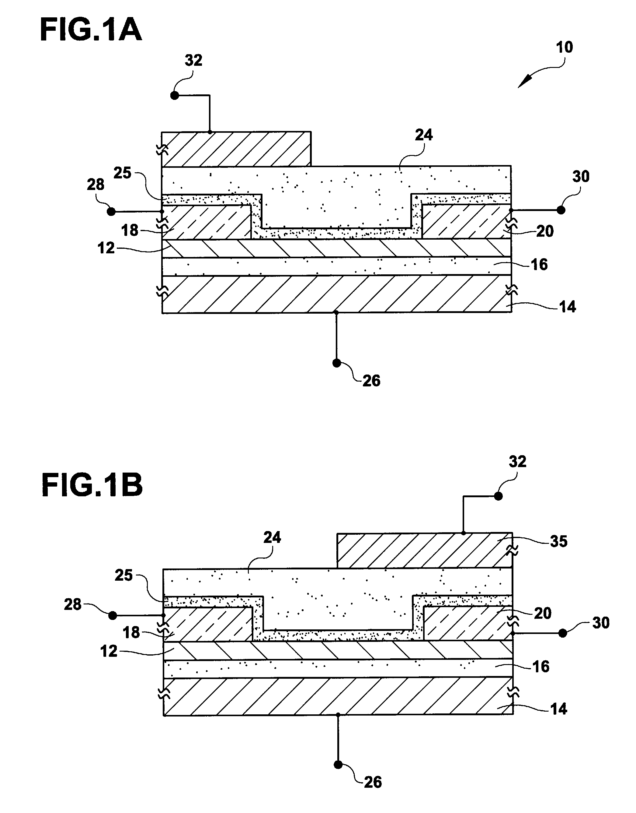
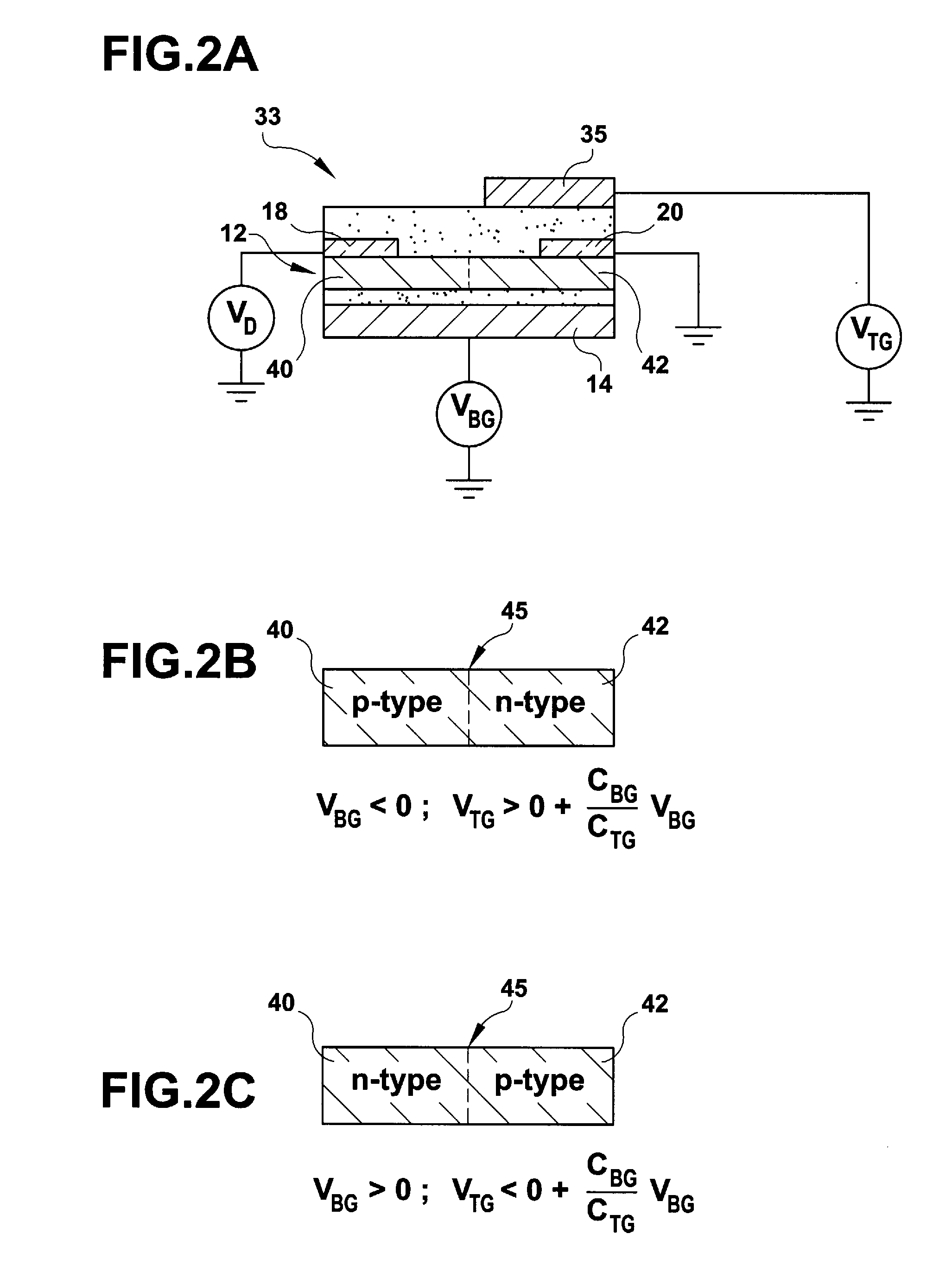
[0081]A graphene device having the configuration of FIG. 1A was microfabricated in accordance with the invention. A 300 nm-thick layer of SiO2 was thermally grown on a degenerately doped Si wafer. Graphene was exfoliated with a taping technique and applied to the oxide surface, and was identified by thin-film interference. Two device electrodes were formed by electron beam lithography and lift off with layers of titanium and gold, of 5 nm and 40 nm in thickness, respectively. A functionalization layer was then formed by the ALD process described above, employing 50 pulsed cycles of NO2 and TMA at room temperature, in the manner given above. The functionalization layer was then stabilized by a 5-cycle ALD process of H2O and TMA at room temperature, also in the manner given above. An oxide layer of Al2O3 was then formed over the stabilized functionalization layer by 300 ALD cycles of pulsed H2O / TMA, at a temperature of about 225° C., yielding an oxide thickness of about 30 nm. To comp...


PUM


Abstract

A graphene device includes a graphene layer and a back gate electrode connected to apply a global electrical bias to the graphene from a first surface of the graphene. At least two graphene device electrodes are each connected to a corresponding and distinct region of the graphene at a second graphene surface. A dielectric layer blanket-coats the second graphene surface and the device electrodes. At least one top gate electrode is disposed on the dielectric layer and extends over a distinct one of the device electrodes and at least a portion of a corresponding graphene region. Each top gate electrode is connected to apply an electrical charge carrier bias to the graphene region over which that top gate electrode extends to produce a selected charge carrier type in that graphene region. Such a carbon structure can be exposed to a beam of electrons to compensate for extrinsic doping of the carbon.

Description

CROSS-REFERENCE TO RELATED APPLICATION[0001]This application claims the benefit of U.S. Provisional Application No. 61 / 125,365, filed Apr. 24, 2008, the entirety of which is hereby incorporated by reference.BACKGROUND OF THE INVENTION[0002]This invention relates to forms of carbon such as graphene and carbon nanotubes, and more particularly relates to microfabrication of carbon-based electronic devices.[0003]Graphene, a single-layer hexagonal lattice of carbon atoms, has recently emerged as a fascinating system for fundamental studies in condensed matter physics, as well as a candidate for novel sensors and post-silicon electronics. Carbon nanotubes (CNTs) and graphene are allotropes of carbon in which the carbon atomic orbitals rearrange to produce a solid in which electrical conduction is possible, as either a metallic or a semiconducting material. The differences in the electrical conduction properties of CNTs and graphene arise solely from the differences in their geometric stru...

Claims


Application Information

Patent Timeline
IPC IPC(8): H01L29/12H01L21/36
CPCB82Y30/00B82Y40/00H01L29/1606C01B31/0484C01B31/0273C01B32/174C01B32/194
Inventor MARCUS, CHARLES M.WILLIAMS, JAMES R.CHURCHILL, HUGH OLEN HILL
Owner PRESIDENT & FELLOWS OF HARVARD COLLEGE
Why Eureka
Try Eureka