Silicon MEMS based two-phase heat transfer device

a heat transfer device and silicon mem technology, applied in the direction of power cables, cables, semiconductor/solid-state device details, etc., can solve the problems of waste heat becoming a significant problem, new chips generating more waste heat, and semiconductor makers struggling to find new ways to cool increasingly powerful chips

Inactive Publication Date: 2007-05-03
UNIVERSITY OF CINCINNATI
View PDF53 Cites 60 Cited by
  • Summary
  • Abstract
  • Description
  • Claims
  • Application Information

AI Technical Summary

Problems solved by technology

Semiconductor makers have been struggling to find new ways to cool increasingly powerful chips.
New chips generate more waste heat because of the increasing numbers of circuits being packed into the chips.
As circuit dimensions shrink into the nanometer realm, waste heat becomes a significant problem.
Increasing power densities, even with smaller switching potentials, causes the chips to warm to unacceptable temperatures.
This condition has lead to ever increasing space consumed by packaging schemes for heat transfer away from the chip-level electronics.
Heat sink and fan assemblies are large, which makes them less useful as the microelectronics industry moves towards thinner and smaller devices.
For instance, while heat sink or fan assemblies are widely used in desktops, laptops cannot accommodate these components.
Another disadvantage of these assemblies is their low convective heat transfer coefficients due to room temperature air acting as the cooling fluid.
Air has low density, low thermal conductivity, and low specific heat, resulting in low heat load carrying capacity.
Heat pipes are limited because they are mostly cylindrical, have vapor and liquid moving counter to one another in the same channel, and often cannot dissipate heat fluxes greater than 10 W / cm2.
Semiconductor makers have been struggling to find new ways to cool their increasingly powerful chips.
For example, Intel recently cancelled its 4-gigahertz Pentium 4 processor because of increasing heat dissipation problems.
However, the consortium between IBM, Toshiba, and Sony plans to use a 16 core processor in forthcoming products that will push the limits of processing power and waste heat mediation.
While waste heat has been a industry-wide problem, cooling solutions will be of utmost importance as circuit dimensions shrink into the nanometer realm causing chips consume more power and give off more heat.

Method used


Image

  • Silicon MEMS based two-phase heat transfer device
  • Silicon MEMS based two-phase heat transfer device
  • Silicon MEMS based two-phase heat transfer device

Examples


Embodiment Construction

[0041] The present invention overcomes problems with the prior art by providing improved thermal transfer devices for removal of heat from a high temperature device, such as integrated circuit chips and microprocessors.

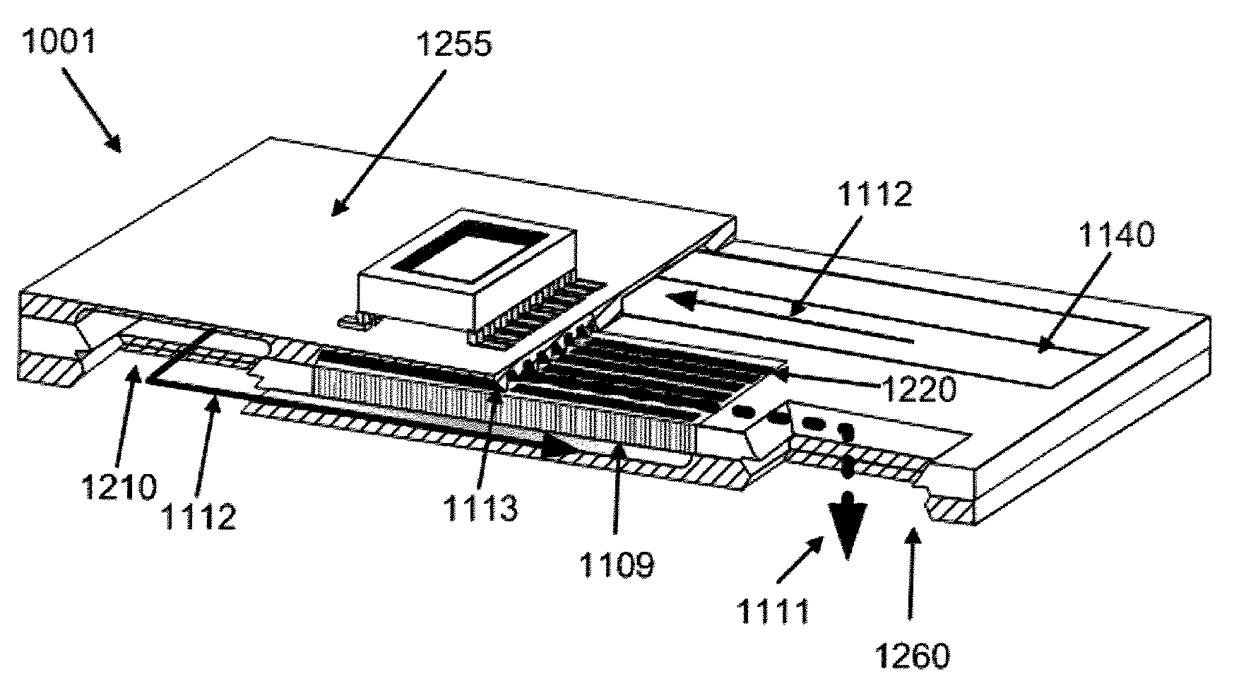
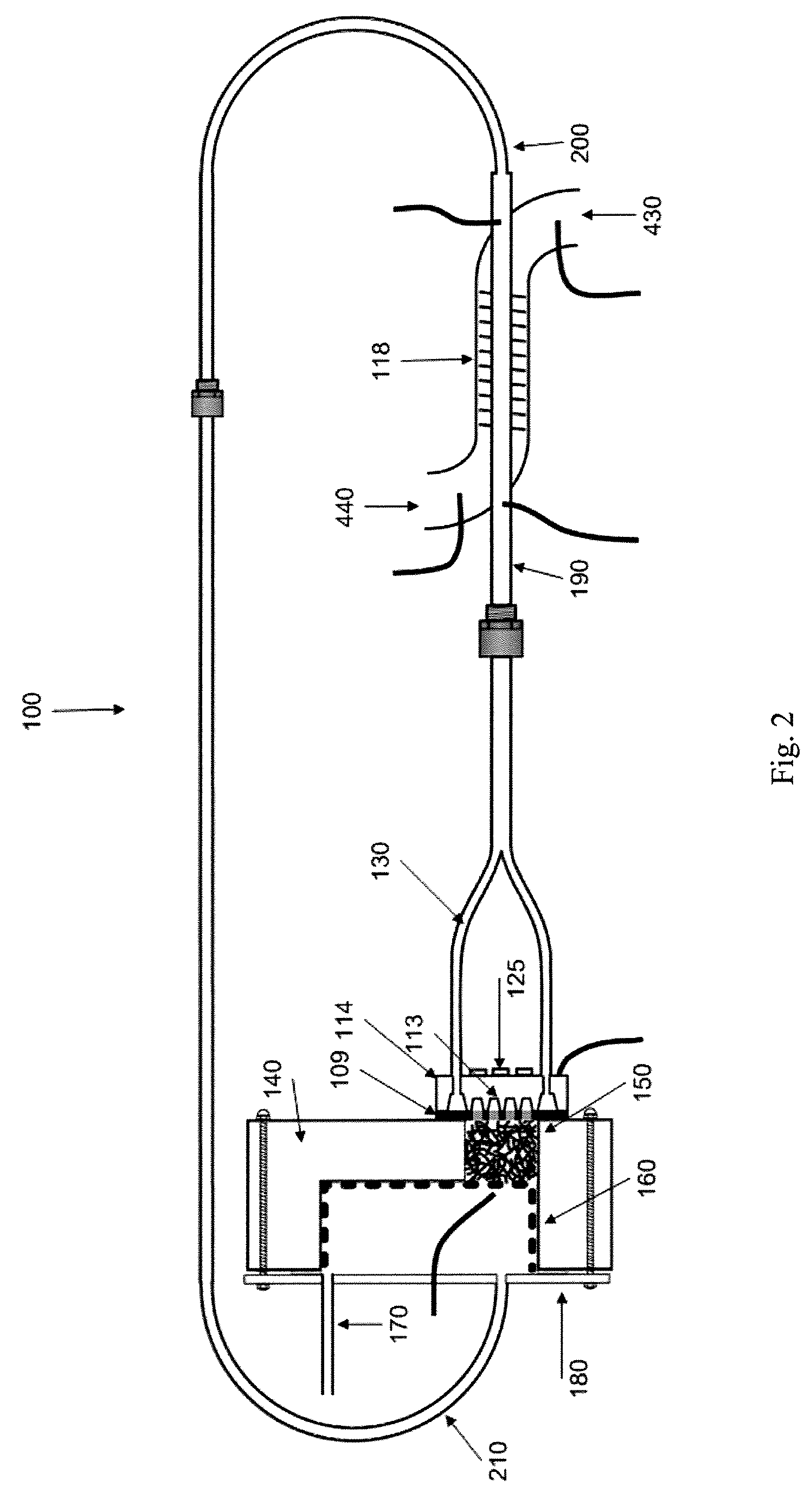
[0042] Two-phase silicon-based thermal transfer devices according to several exemplary embodiments of the present invention are described below. One embodiment of the basic construction of the thermal transfer device 100 is shown in FIG. 2. This embodiment includes an evaporator 101 connected to a condenser 118. The evaporator 101, passage ways 130, 210 and the condenser 118 form a closed loop with hermetic sealing. After evacuating the device, using the fill / vacuum port 170, a liquid working fluid 112 is introduced via fill / vacuum port 170. The amount of liquid working fluid 112 introduced is often a fraction of the total loop internal volume. A heat source (e.g., an integrated or attached semiconductor chip or other device) 125 is cooled at the evaporator 101. The ...


PUM

PropertyMeasurementUnit
convective heat transfer coefficientaaaaaaaaaa
porosityaaaaaaaaaa
diametersaaaaaaaaaa

Abstract

The present invention is a MEMS-based two-phase LHP (loop heat pipe) and CPL (capillary pumped loop) using semiconductor grade silicon and microlithographic/anisotrophic etching techniques to achieve a planar configuration. The principal working material is silicon (and compatible borosilicate glass where necessary), particularly compatible with the cooling needs for electronic and computer chips and package cooling. The microloop heat pipes (μLHP™) utilize cutting edge microfabrication techniques. The device has no pump or moving parts, and is capable of moving heat at high power densities, using revolutionary coherent porous silicon (CPS) wicks. The CPS wicks minimize packaging thermal mismatch stress and improves strength-to-weight ratio. Also burst-through pressures can be controlled as the diameter of the coherent pores can be controlled on a sub-micron scale. The two phase planar operation provides extremely low specific thermal resistance (20-60W/cm2). The operation is dependent upon a unique micropatterened CPS wick which contains up to millions per square centimeter of stacked uniform micro-through-capillaries in semiconductor-grade silicon, which serve as the capillary “engine,” as opposed to the stochastic distribution of pores in the typical heat pipe wick. As with all heat pipes, cooling occurs by virtue of the extraction of heat by the latent heat of phase change of the operating fluid into vapor. In the cooling of a laptop computer processor the device could be attached to the processor during laptop assembly. Consistent with efforts to miniaturize electronics components, the current invention can be directly integrated with a unpackaged chip. For applications requiring larger cooling surface areas, the planar evaporators can be spread out in a matrix and integrally connected through properly sized manifold systems.

Description

CROSS-REFERENCE TO RELATED APPLICATIONS [0001] This application claims the benefit of provisional application Ser. No. 60 / 718,258 that was filed on Sep. 16, 2005, the content of which is incorporated by reference into this application as if fully set forth herein.FIELD OF THE INVENTION [0002] This invention generally relates to methods and devices for heat transfer and dissipation om various applications (e.g., the microelectronics field) and, more specifically, to two-phase heat transfer devices fabricated by microelectromechanical systems (MEMS) technology for thermal management and cooling of semiconductor devices. The device(s) may also be applied to any application where heat is to be removed from an appropriate surface. BACKGROUND OF THE INVENTION [0003] Semiconductor makers have been struggling to find new ways to cool increasingly powerful chips. New chips generate more waste heat because of the increasing numbers of circuits being packed into the chips. As circuit dimension...

Claims


Application Information

Patent Timeline
Patent Type & Authority Applications(United States)
IPC IPC(8): F28D15/00H05K7/20
CPCF28D15/043H01L23/427H01L2924/09701Y10T29/49396Y10S165/218H01L2924/0002H01L2924/00
Inventor HENDERSON, H. THURMANSHUJA, AHMEDPARIMI, SRINIVASGERNER, FRANK M.MEDIS, PRAVEEN
Owner UNIVERSITY OF CINCINNATI
Why Eureka
Try Eureka