Semiconductor device and method of manufacturing the same

a semiconductor device and active layer technology, applied in the field of semiconductor devices, can solve the problems of low light usage, uneven color, and reduced device sensitivity, and achieve the effects of reducing the variation of the thickness of the semiconductor device formed in the active layer, reducing the accuracy of the end point of silicon wafer thinning, and reducing the thickness of the semiconductor devi

Inactive Publication Date: 2011-04-21
SUMCO CORP
View PDF6 Cites 43 Cited by
  • Summary
  • Abstract
  • Description
  • Claims
  • Application Information

AI Technical Summary

Benefits of technology

[0031]According to the above-mentioned semiconductor device, the thinning stop layer is formed along the entire plane of the wafer, by implanting oxygen ions and subsequent heat-treating, in the surface layer of the silicon wafer having an epitaxial film. The thinning stop layer is an imperfect buried oxide film having a mixture of silicon grains and the silicon oxide. Because of this, the, the reliability of the accuracy of the end point of silicon wafer thinning is higher than that of a thinning using the conventional deep trench structure as an end point detector. As a result, variation of the thickness of the semiconductor device formed in an active layer can be reduced.
[0032]According to the method of manufacturing the semicondu

Problems solved by technology

It is known that the sensitivity of the device is reduced because of a low usage of light resulted from the obstruction of the penetrating light by the multilayer interconnections.
With variations in the thickness of the solid-state imaging sensor, it may cause inconsistent incident intensity of light with respect to each CMOS solid-state imaging sensor, generating uneven color.
However, in the method of thinning the silicon wafer using the end point detector having the deep trench structure as disclosed in Japanese Unexamined Patent Application Publication No. 2005-353996, the amount of dry etching for the surface layer of the wafer is not u

Method used


Image

  • Semiconductor device and method of manufacturing the same
  • Semiconductor device and method of manufacturing the same
  • Semiconductor device and method of manufacturing the same

Examples


first embodiment

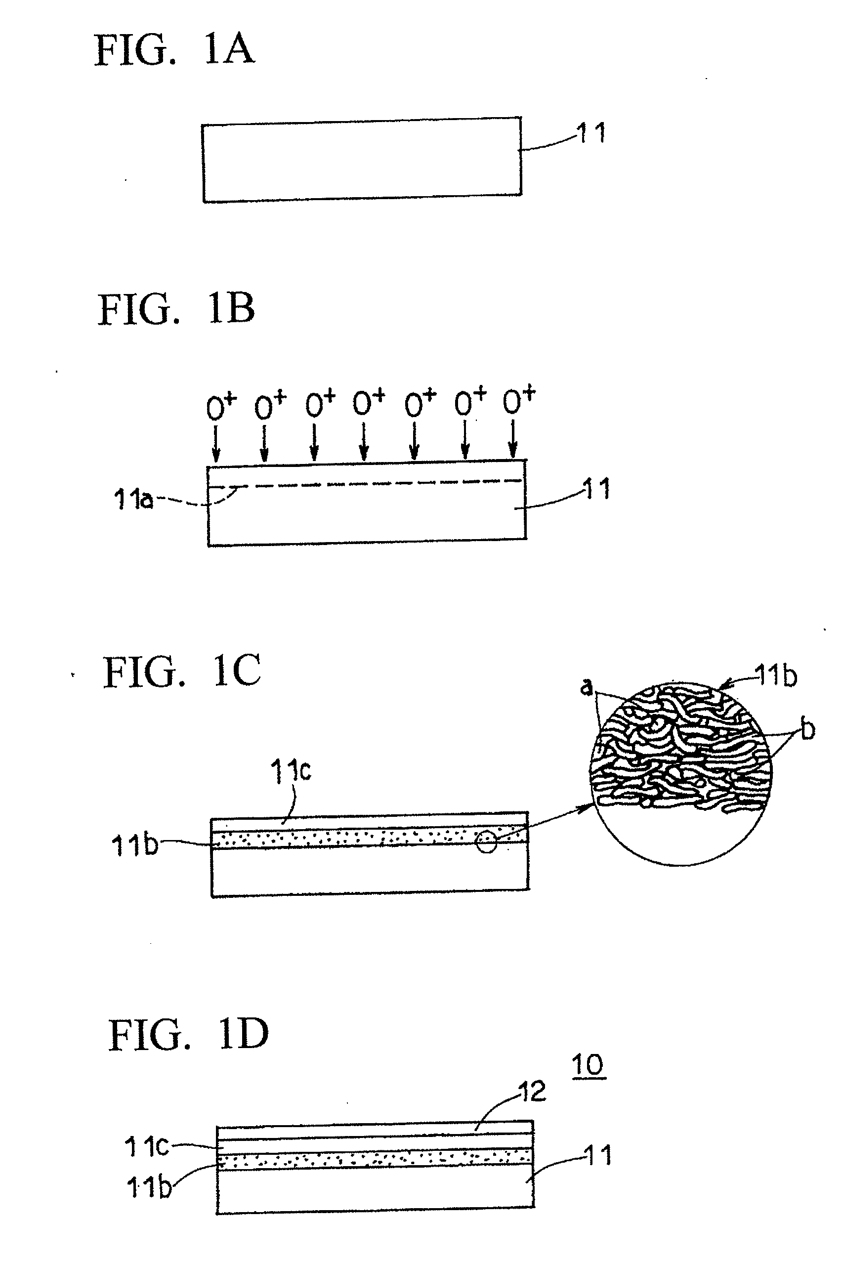
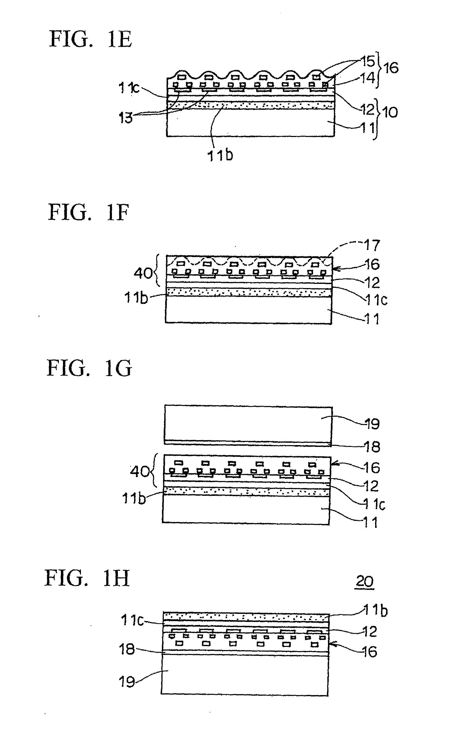
[0045]In a method of manufacturing a semiconductor device of the present invention, first, oxygen ions are implanted from the surface of a silicon wafer in a step of ion-implanting. An ion-implanted layer is formed in the surface layer of the silicon wafer. In a step of heat-treating and film forming, the ion-implanted layer is heat treated, and an epitaxial film is formed on the surface of the silicon wafer, after the step of ion-implanting. A thinning stop layer having a mixture of silicon grains and a silicon oxide is formed along the entire plane of the silicon wafer by the heat treatment. In addition, an active layer is formed between the surface side of the silicon wafer and the thinning stop layer. After that, in a step of forming a semiconductor device, a semiconductor device is formed in the epitaxial film. Next, in a step of bonding, a support substrate is bonded to the surface of the epitaxial film to produce a bonded wafer. After bonding, in a step of thinning, the silic...

second embodiment

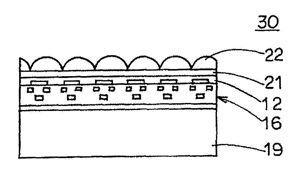
[0076]A semiconductor device which is the invention includes: a silicon wafer; a thinning stop layer having a mixture of silicon grains and a silicon oxide, formed in the surface layer of the silicon wafer along the entire plane of the wafer by implanting oxygen ions into the silicon wafer from the surface thereof, and then heat-treating the silicon wafer; an active layer formed between the surface side of the silicon wafer and the thinning stop layer; an epitaxial film formed on the surface of the active layer; a semiconductor device formed in the epitaxial film; and a support substrate bonded to the surface of the epitaxial film, wherein the silicon wafer and the thinning stop layer are thinned from a back side of the silicon wafer, by at least one of grinding, polishing, and wet-etching until a remaining thickness thereof to be 10 to 100 μm, and then further thinned by dry-etching as a finishing process.

[0077]According to the semiconductor device of the second embodiment of the p...


PUM


Abstract

A semiconductor device and a method of manufacturing the same capable of reducing variations in the thickness of a semiconductor device are provided. The amount of oxygen implanted ions is less than the amount of implanted oxygen ions in the conventional epitaxial SIMOX wafers. Oxygen is ion-implanted into the surface layer of a silicon wafer from the surface of the wafer. Then, by heat treating the wafer, a thinning stop layer, which is an imperfect buried oxide film, is formed along the entire plane of the wafer. As a result, variation of the thickness of the semiconductor device formed in an active layer can be reduced, since the, the reliability of the accuracy of the end point of silicon wafer thinning is higher than that of a thinning using the conventional deep trench structure as an end point detector.

Description

BACKGROUND OF THE INVENTION[0001]1. Field of the Invention[0002]The present invention relates to a semiconductor device and a method of manufacturing the same. More specifically, it relates to a semiconductor device formed on a silicon wafer that is required to be thinned, and a method of manufacturing the same.[0003]Priority is claimed on Japanese Patent Application No. 2009-239673, filed Oct. 16, 2009, the content of which is incorporated herein by reference.[0004]2. Description of Related Art[0005]For example, in a frontside illuminated CMOS solid-state imaging sensor, which is one of semiconductor device, multilayer interconnections exist in a path of light to be irradiated, particularly, in the light path of angled light in the peripheral portion of the effective pixel area. It is known that the sensitivity of the device is reduced because of a low usage of light resulted from the obstruction of the penetrating light by the multilayer interconnections. Consequently, as the rela...

Claims


Application Information

Patent Timeline
IPC IPC(8): H01L29/02H01L21/762
CPCH01L21/26533H01L27/1464H01L27/14692H01L21/76256
Inventor NONOGAKI, YOSHIHISA
Owner SUMCO CORP
Why Eureka
Try Eureka