Thin film transistor and display device

a thin film transistor and display device technology, applied in the direction of transistors, semiconductor devices, electrical appliances, etc., can solve the problems of increased leak current and reduced threshold voltage, and achieve the effects of clear display, reduced leak current generation, and improved luminan

Inactive Publication Date: 2011-04-28
JOLED INC
View PDF1 Cites 127 Cited by
  • Summary
  • Abstract
  • Description
  • Claims
  • Application Information

AI Technical Summary

Benefits of technology

[0011]According to the thin film transistor, the method of manufacturing the thin film transistor, and the display device of the present invention, since the one or the plurality of protective films are provided so as to face the channel region of the oxide semiconductor film in which the channel region is formed, and at least one protective film of these contains the aluminum oxide, the entry of the hydrogen or the like into the oxide semiconductor film is suppressed, and generation of a leak current may be suppressed. Further, thereby, luminance is improved, and a clear display is available in the display device.

Problems solved by technology

Thus, for example, in the case where the zinc oxide is used for the thin film transistor, the operation is a normally-on type operation in which a drain current is allowed to flow even when a gate voltage is not applied, that is, a depression type operation, and there is an issue that a threshold voltage is reduced with an increase of a defect level, and a leak current is increased.

Method used


Image

  • Thin film transistor and display device
  • Thin film transistor and display device
  • Thin film transistor and display device

Examples


first embodiment

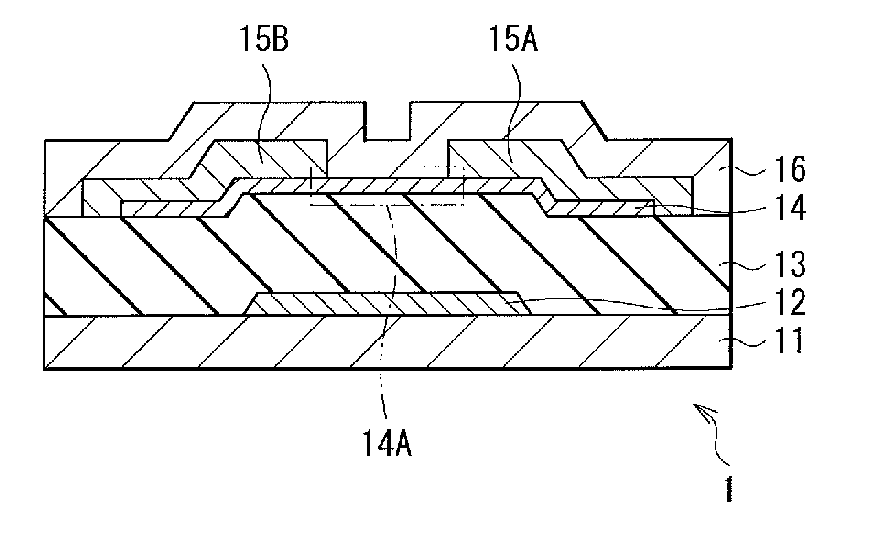
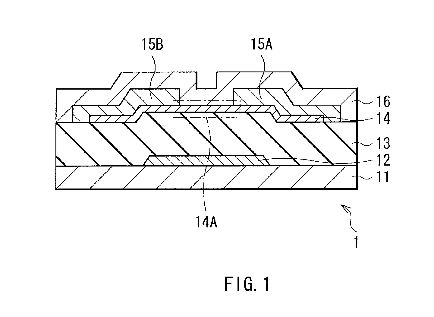
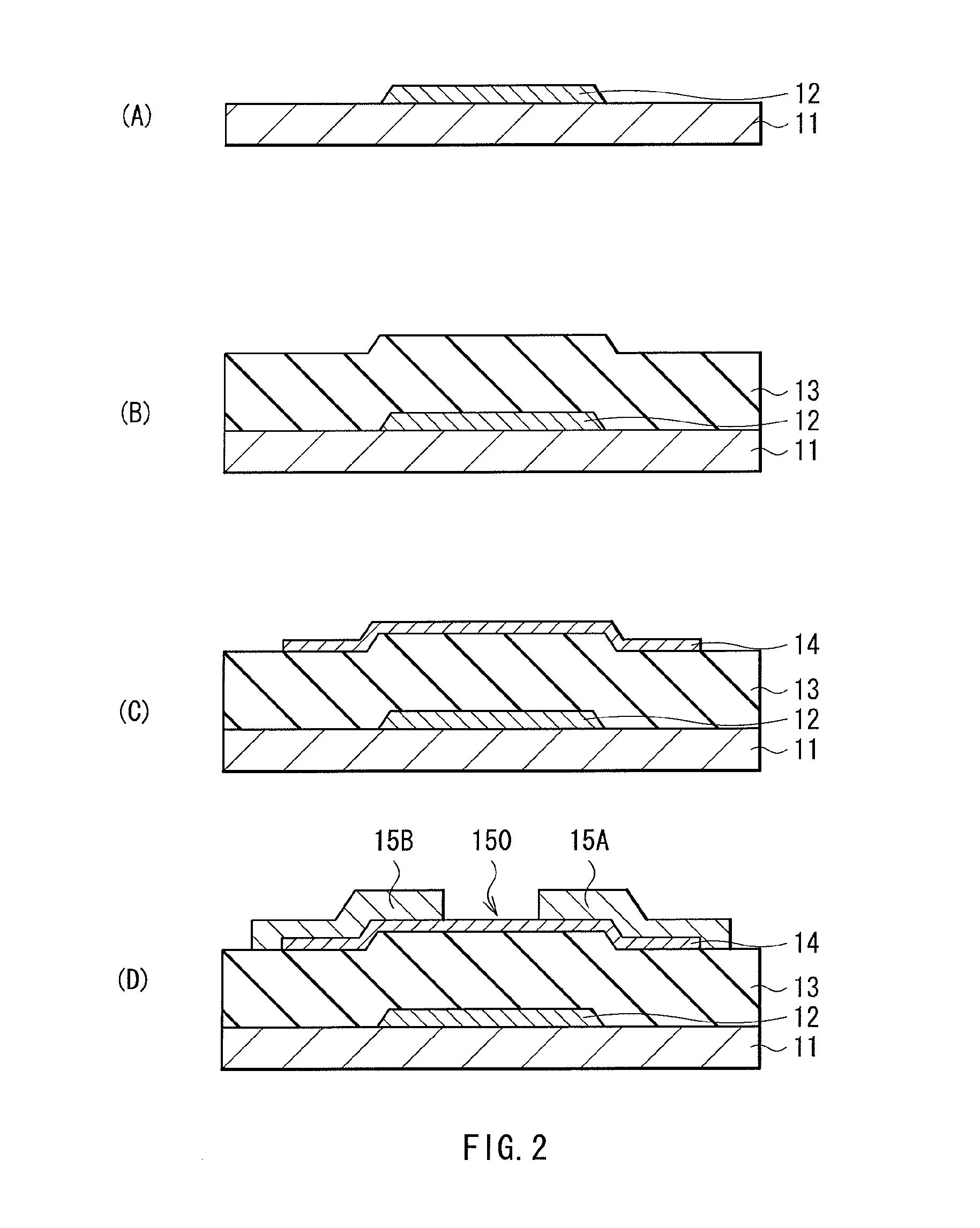
[0025]FIG. 1 illustrates the cross-sectional structure of a thin film transistor 1 according to a first embodiment of the present invention. The thin film transistor 1 has, for example, a bottom-gate type structure, and an oxide semiconductor is used for a channel region (active layer). The thin film transistor 1 includes a gate electrode 12 on a substrate 11 which is made of glass, plastic, or the like, and a gate insulating film 13 is provided so as to cover the gate electrode 12 and the substrate 11. An oxide semiconductor film 14 is formed in a region corresponding to the gate electrode 12 on the gate insulating film 13, and a pair of electrodes (a source electrode 15A and a drain electrode 15B) is provided on the oxide semiconductor film 14 with a predetermined interval in between. A protective film 16 is formed over the whole surface of the substrate 11, so as to cover a channel region 14A of the oxide semiconductor film 14, the source electrode 15A, and the drain electrode 15...

second embodiment

[0043]FIG. 3 illustrates the cross-sectional structure of a thin film transistor 2 according to a second embodiment of the present invention. Like the above-described first embodiment, the thin film transistor 2 has the bottom-gate type structure, and the oxide semiconductor is used for the channel region (active layer). Hereinafter, same reference numerals will be used for components identical to those of the above-described first embodiment, and the description will be appropriately omitted.

[0044]In the thin film transistor 2, the gate electrode 12, the gate insulating film 13, and the oxide semiconductor film 14 are provided on the substrate 11. In this embodiment, a channel protective film 17 (first protective film) is formed on the top face of the oxide semiconductor film 14, and a protective film 18 (second protective film) is formed so as to cover the top face of this channel protective film 17 and the side face of the oxide semiconductor film 14. Apertures 170A and 170B are ...

third embodiment

[0054]FIG. 5 illustrates the cross-sectional structure of a thin film transistor 3 according to a third embodiment of the present invention. Like the above-described first embodiment, the thin film transistor 3 has the bottom gate type structure, and the oxide semiconductor is used for the channel region (active layer). Hereinafter, same reference numerals will be used for components identical to those of the above-described first embodiment, and the description will be appropriately omitted.

[0055]In the thin film transistor 3, the gate electrode 12, the gate insulating film 13, and the oxide semiconductor film 14 are provided on the substrate 11. A channel protective film 20 (first protective film) is formed in the region corresponding to the channel region 14A on the oxide semiconductor film 14. In this embodiment, a source electrode 21A and a drain electrode 21B are provided on the oxide semiconductor film 14 so as to cover end portions of the channel protective film 20. Further,...


PUM


Abstract

There is provided a thin film transistor capable of suppressing generation of a leak current in an oxide semiconductor film. A thin film transistor 1 includes a gate electrode 12 on a substrate 11, and includes a gate insulating film 13 so as to cover the gate electrode 12 and the substrate 11. An oxide semiconductor film 14 is formed in a region corresponding to the gate electrode 12 on the gate insulating film 13, and a source electrode 15A and a drain electrode 15B are provided with a predetermined interval in between on the oxide semiconductor film 14. A protective film 16 is formed over a whole surface of the substrate 11 so as to cover a channel region 14A of the oxide semiconductor film 14, the source electrode 15A, and the drain electrode 15B. The protective film 16 is composed of an aluminum oxide film, and this aluminum oxide film is formed by an atomic layer deposition method. An entry of hydrogen into the oxide semiconductor film 14 is suppressed by the protective film 16.

Description

TECHNICAL FIELD[0001]The present invention relates to a thin film transistor using an oxide semiconductor film, and a display device using the thin film transistor.BACKGROUND ART[0002]In recent years, for the purpose of application to an electronic device such as a thin film transistor (TFT: Thin Film Transistor), a light emitting device, and a transparent conductive film, study and development of a semiconductor thin film layer (hereinafter, referred to as an oxide semiconductor film) using zinc oxide, indium gallium zinc oxide, or the like have been activated. It is known that such an oxide semiconductor film has the high electron mobility, and the excellent electric characteristics, in comparison with the case where amorphous silicon (α-Si) which is typically used for a liquid crystal display or the like is used. Further, there is an advantage that the high mobility may be expected even at a low temperature around a room temperature, or the like, and development has been actively...

Claims


Application Information

Patent Timeline
Patent Type & Authority Applications(United States)
IPC IPC(8): H01L29/786H01L21/44H01L33/28
CPCH01L29/7869H01L29/66742H01L29/78606
Inventor MOROSAWA, NARIHIROARAI, TOSHIAKI
Owner JOLED INC
Why Eureka
Try Eureka