Printed Material Constrained By Well Structures And Devices Including Same

a printing material and well structure technology, applied in the direction of basic electric elements, semiconductor devices, electrical equipment, etc., can solve the problems of cross contamination of devices to devices, short circuits between devices, and tendency to spread after, so as to improve device-to-device isolation

Active Publication Date: 2011-04-28
XEROX CORP
View PDF87 Cites 17 Cited by
  • Summary
  • Abstract
  • Description
  • Claims
  • Application Information

AI Technical Summary

Benefits of technology

[0011]Accordingly, the present disclosure provides methods for manufacturing micro-electronic, opto-electronic, bio-electronic, or similar devices employing digital lithography, and the devices so manufactured, which have improved device-to-device isolation as compared to methods and devices previously produced by digital lithography.

Problems solved by technology

Digital lithography directly deposits patterned material onto a substrate in place of the delicate and time-consuming photolithography processes used in conventional manufacturing processes.
However, one disadvantage of digital lithography is that since the printed material is deposited in liquid form, it tends to spread after deposition and prior to solidification.
When printing devices close together, for example less that 20-40 μm (micrometers) edge-to-edge, the droplet spreading can result in device-to-device short circuit (e.g., when forming electronic devices such as transistors), or device-to-device cross contamination (e.g., when forming an array of biological test units).
While digital lithography has been used to isolate adjacent structures, such as wells for color filter material in a color filter for a flat panel display and the like, heretofore no device designs have successfully included printed well structures in forming active electronic devices, forming structures over active device layers, nor forming structures to confine the deposition of active device material.

Method used


Image

  • Printed Material Constrained By Well Structures And Devices Including Same
  • Printed Material Constrained By Well Structures And Devices Including Same
  • Printed Material Constrained By Well Structures And Devices Including Same

Examples


first embodiment

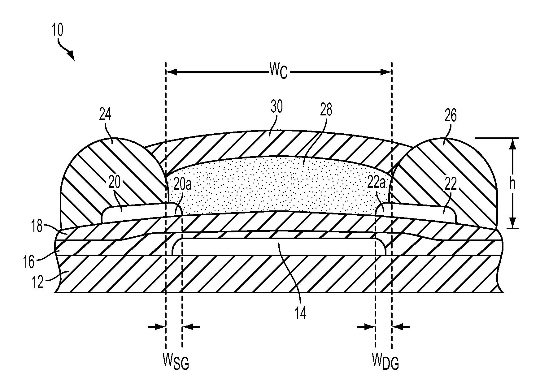
[0026]According to this disclosure, illustrated in FIG. 1, a bottom-gate transistor device is fabricated. The embodiment makes extensive use of digital lithography, digital printing or laser transfer processes. Spreading of materials deposited, for example by a digital lithography process, is reduced so that more compact devices are possible, smaller pitch arrays are possible, and device-to-device shorting is eliminated. The embodiments described herein related to the formation of active electronic devices, such as electronic switching elements, as opposed to passive elements, such as electrical filters and the like.

[0027]With reference to FIG. 1, the formation of a device 10 begins with preparation of a suitable substrate 12. Many different types of substrates may be employed, since growth is not epitaxial from the substrate. Examples of substrate materials include ceramics, polymers, crystalline materials, metals, etc., and may be rigid or flexible. In the case of conductive subst...

embodiment 150

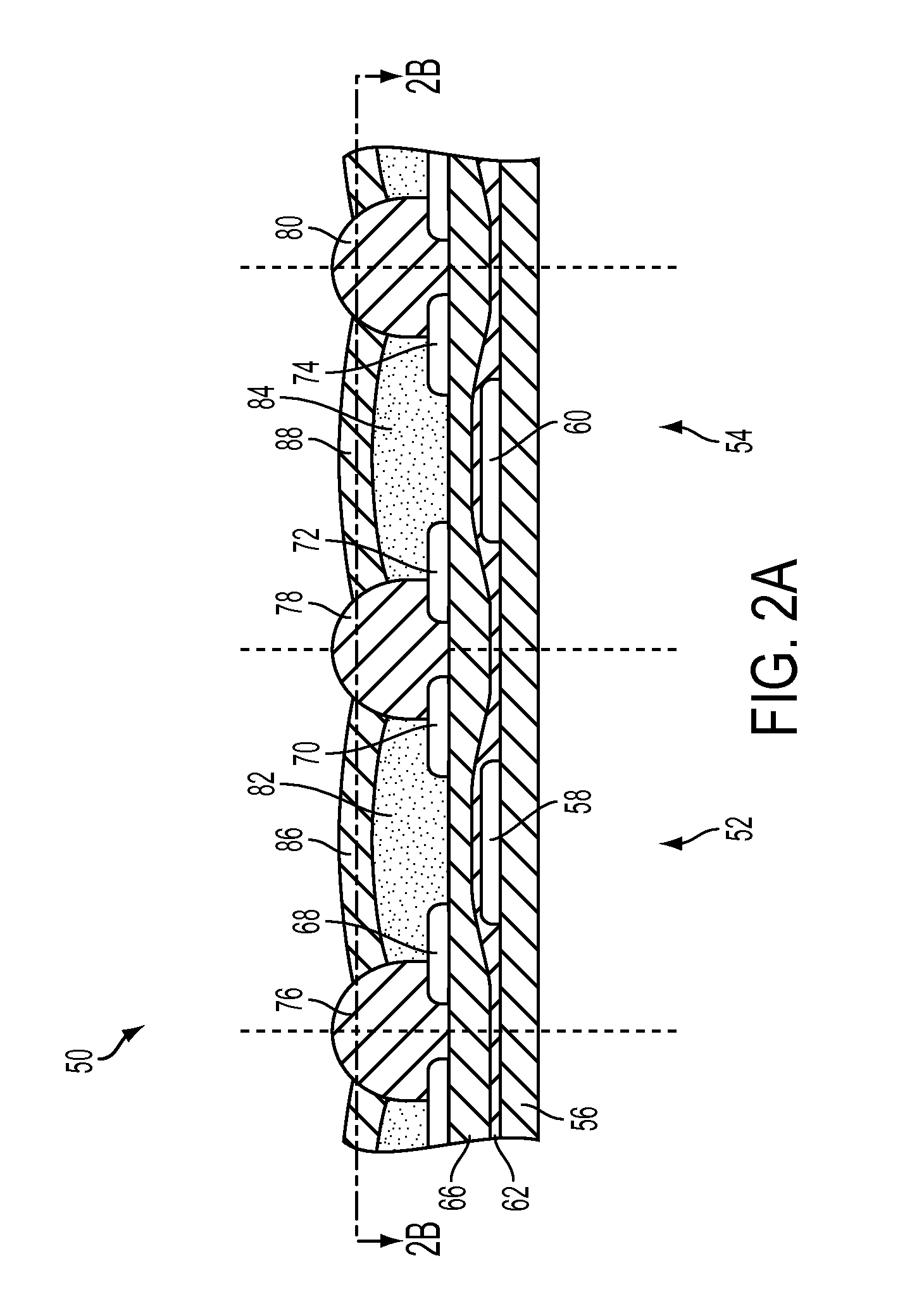
[0058]Furthermore, the above disclosure has been based on forming a functional layer below source and drain electrodes. However, it is possible to first form the source and drain electrodes, then form the functional layer thereover. In this case, the functional layer has to be very thin to allow electron tunneling through the layer and / or to exhibit a sufficient population of pinholes for an electrical contact to form between source / drain electrodes and a semiconductor layer formed between the walls thereover. An embodiment 150 having the functional layer 18 formed over electrodes 20, 22 is illustrated in FIG. 5. Again, an overlap 20a, 22a is provided between a gate electrode 14 and a portion of source electrode 20a and drain electrode 22a. The method for forming such a device is substantially as described above, with the order of forming the source and drain electrodes and the functional layer simply reversed.


PUM


Abstract

A first patterned contact layer, for example a gate electrode, is formed over an insulative substrate. Insulating and functional layers are formed at least over the first patterned contact layer. A second patterned contact layer, for example source / drain electrodes, is formed over the functional layer. Insulative material is then selectively deposited over at least a portion of the second patterned contact layer to form first and second wall structures such that at least a portion of the second patterned contact layer is exposed, the first and second wall structures defining a well therebetween. Electrically conductive or semiconductive material is deposited within the well, for example by jet-printing, such that the first and second wall structures confine the conductive or semiconductive material and prevent spreading and electrical shorting to adjacent devices. The conductive or semiconductive material is in electrical contact with the exposed portion of the second patterned contact layer to form, e.g., an operative transistor.

Description

STATEMENT REGARDING FEDERALLY SPONSORED RESEARCH AND DEVELOPMENT[0001]The U.S. Government has a fully paid-up license in this disclosure and the right in limited circumstances to require the patent owner to license others on reasonable terms as provided for by the terms of contract number W81XWH-08-C-0065 DARPA-SENSOR TAPE, awarded by the Defense Advanced Research Projects Agency (DARPA).BACKGROUND[0002]1. Field of the Invention[0003]This invention relates generally to electronic device fabrication, and more particularly to a method employing a printed mask to form active device elements by a printing process such that the printed mask controls dimensions of the active device elements.[0004]2. Description of the Prior Art[0005]Digital lithography is a maturing technology designed to reduce the costs associated with photolithographic processes, used often in the fabrication of micro-electronic devices, integrated circuits, and related structures. Digital lithography directly deposits...

Claims


Application Information

Patent Timeline
Patent Type & Authority Applications(United States)
IPC IPC(8): H01L29/78H01L21/336
CPCH01L29/78684H01L29/7869H01L51/0004H01L29/66742H01L21/02288H01L21/02628H01L29/66772H01L27/1292H01L21/368H01L21/02488H01L21/02521H01L21/02623H10K71/13H01L21/38
Inventor DANIEL, JURGEN H.ARIAS, ANA CLAUDIA
Owner XEROX CORP
Why Eureka
Try Eureka