Semiconductor device, system with semiconductor device, and calibration method

a semiconductor device and semiconductor technology, applied in the field of semiconductor device and system including semiconductor device, can solve the problems of large electrical power consumption of the system when the calibration is performed, the calibration method and the calibration process of a related semiconductor device cannot complete the impedance matching within the calibration period. , to achieve the effect of reducing the variation of the impedance, shortening the period of time, and reducing the electric power consumption of the system

Inactive Publication Date: 2011-05-05
LONGITUDE SEMICON S A R L
View PDF28 Cites 48 Cited by
  • Summary
  • Abstract
  • Description
  • Claims
  • Application Information

AI Technical Summary

Benefits of technology

[0012]According to the present invention, a calibration operation is performed under a voltage condition that allows the maximum current to flow through the output driver. Therefore, the adjusted impedance precisely coincides with the impedance at the time when the output driver actually operates. Therefore, variations of the impedance can be reduced between a plurality of output drivers. Furthermore, with the parameter table obtained by a calibration test conducted at the time of vendor's shipment, a calibration operation can be performed with reference to only the table in a system on which the semiconductor device has been mounted. Accordingly, it is possible to shorten a period of time required for a calibration operation and to decrease the electric power consumption in the system. Since this results in a reduction of noise, it is possible to avoid a situation in which impedance matching cannot be completed. Moreover, the degree of integration of a substrate can be improved while the number of parts can be reduced. According to the present invention, at least one of those advantages can be obtained.

Problems solved by technology

Moreover, according to the calibration method of a related semiconductor device, the system consumes much electric power when the calibration is performed.
Furthermore, according to the calibration method of a related semiconductor device, the calibration requires a long period of time until it is finished.
Moreover, in some cases, the calibration method of a related semiconductor device cannot complete impedance matching within the period of the calibration due to external / internal factors such as noise caused at the time of the calibration.

Method used


Image

  • Semiconductor device, system with semiconductor device, and calibration method
  • Semiconductor device, system with semiconductor device, and calibration method
  • Semiconductor device, system with semiconductor device, and calibration method

Examples


first embodiment

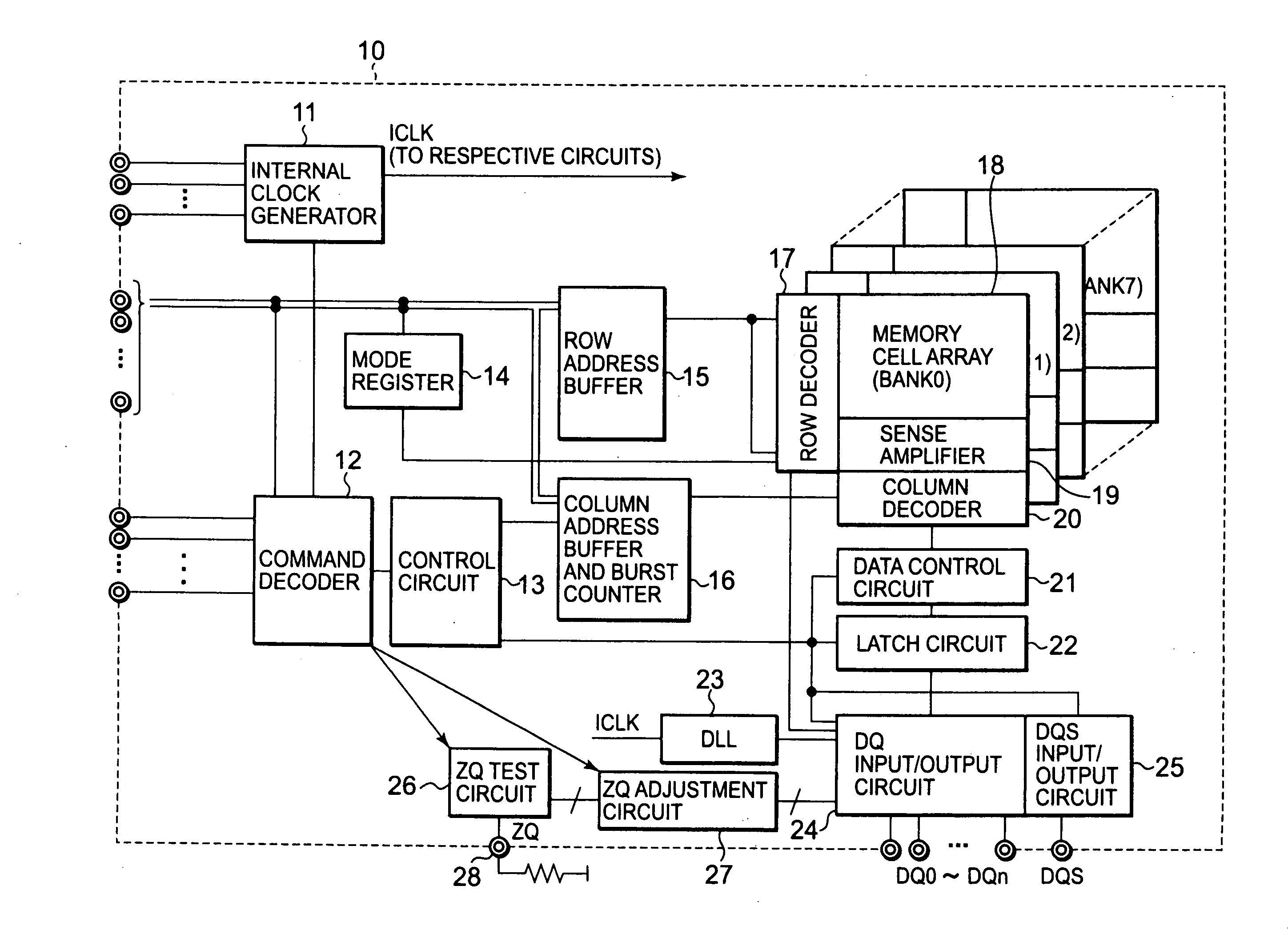
[0041]FIG. 1 shows an example of a configuration of a semiconductor device according to the present invention. A semiconductor device 10 shown in FIG. 1 is a dynamic random access memory (DRAM). The semiconductor device 10 includes an internal clock generator 11, a command decoder 12, a control circuit 13, a mode register 14, a row address buffer 15, a column address buffer and burst counter 16, row decoders 17, memory cell arrays 18, sense amplifiers. 19, column decoders 20, a data control circuit 21, a latch circuit 22, a delay locked loop (DLL) 23, a data signal (DQ) input / output circuit 24, a data strobe signal (DQS) input / output circuit 25, a zero quotient (ZQ) test circuit 26, and a ZQ adjustment circuit 27.

[0042]The data signal (DQ) input / output circuit 24 includes output transistors (not shown) respectively connected to a plurality of external terminals DQi (first external terminals) for outputting internal data from the DQ input / output circuit 24 and input transistors (not ...

second embodiment

[0116]Next, a system according to the present invention will be described below with reference to FIG. 15.

[0117]The system of FIG. 15 includes a plurality of first semiconductor devices 1510 and a second semiconductor device 1520. The first semiconductors devices 1510 are connected to the second semiconductor device 1520 by a command bus 1531 and a data input / output (I / O) bus 1532.

[0118]Each of the first semiconductor devices 1510 includes memory cells 1511, a back-end interface 1512, and a front-end interface 1513.

[0119]The second semiconductor device 1520 includes a control signal issuance circuit 1521 and a data processing circuit 1522. The second semiconductor device 1520 serves as a controller for controlling the first semiconductor devices 1510. Furthermore, the second semiconductor device 1520 has other circuits not shown in the system and interfaces for circuits outside of the system. The second semiconductor device 1520 controls the entire system.

[0120]The front-end interfa...

third embodiment

[0122]Next, a system according to the present invention will be described below with reference to FIG. 16. The following description is focused on differences between this system and the system shown in FIG. 15.

[0123]The system of FIG. 16 includes first semiconductor devices 1510-1, each of which has no ZQ adjustment circuit 27. The ZQ test circuit 26 of each of the first semiconductor devices 1510-1 is connected to the ZQ adjustment circuit 27 of the second semiconductor device (controller) 1520. That is, in the system according to the third embodiment, the ZQ adjustment circuit 27 of one of the semiconductor devices is used in common by other semiconductor devices.

[0124]Impedance adjustment of the output driver of each of the first semiconductor devices 1510-1 is performed with control information stored in a memory unit of the ZQ adjustment circuit 27 of the second semiconductor device 1520. In other words, the impedance of the output driver included in the front-end interface of...


PUM


Abstract

Variations of the impedance of each output driver of a semiconductor device can be reduced, and high-speed calibration is achieved. A calibration circuit including a replica circuit having the same configuration as each pull-up circuit or pull-down circuit included in an output driver of a semiconductor device is provided within a chip. During a first calibration operation, the replica circuit is provided with voltage conditions that allow the maximum current to flow through the output driver so that an impedance of the replica circuit is equal to a value of an external resistor. During a second calibration operation, table parameters obtained in the first calibration operation are used to adjust the impedance of the output driver without use of the replica circuit.

Description

[0001]This application is based upon and claims the benefit of priority from Japanese patent application No. 2009-253694, filed on Nov. 5, 2009, the disclosure of which is incorporated herein in its entirety by reference.BACKGROUND OF THE INVENTION[0002]1. Field of the Invention[0003]The present invention relates to a semiconductor device, a system including a semiconductor device, and calibration thereof. More particularly, the present invention relates to a calibration method and a calibration circuit for controlling an impedance of an output driver connected to an external terminal.[0004]2. Description of Related Art[0005]A semiconductor device according to a related art includes a calibration circuit therein so as to control an impedance of each output driver formed by transistors. The calibration circuit includes a replica circuit which is identical in structure to the output driver of the semiconductor device. The replica circuit is connected to an external terminal, to which ...

Claims


Application Information

Patent Timeline
Patent Type & Authority Applications(United States)
IPC IPC(8): G05F1/10
CPCH04L25/0278H03K19/0005G11C7/1057G11C7/1072G11C7/1084G11C29/022G11C29/025G11C29/028G11C29/12005G11C2029/4402G11C2207/2254
Inventor RIHO, YOSHIRO
Owner LONGITUDE SEMICON S A R L
Why Eureka
Try Eureka