Sensor for quantitative measurement of electromechanical properties and microstructure of nano-materials and method for making the same

Active Publication Date: 2011-05-05
BEIJING UNIV OF TECH
View PDF9 Cites 17 Cited by
  • Summary
  • Abstract
  • Description
  • Claims
  • Application Information

AI Technical Summary

Benefits of technology

The features and advantage of the present invention will be apparent from the following detailed descriptions of the preferred aspects of the invention in conjunction with the accompanying drawings wherein:
FIG. 1a-1j, illustrates production flow chart of the present invention of the sensor
FIG. 2, illustrates sk

Problems solved by technology

But at present the TEM grid is effective only for the static testing, and not for in situ manipulation and dynamic quantitative testing the properties of nano-material at the nano-scale even to atomic scale level.
But installing these devices inside the TEM holder that causes the holder can tilt a small angle and only a single axis tilting because of the narrow pole-piece gap.
However, atomic-scale lattice resolution of a crystal is only achieved when a low-indexed zone axis of a crystal is precisely aligned parallel to the electron beam.
This condition is difficult to fulfill in these in situ

Method used


Image

  • Sensor for quantitative measurement of electromechanical properties and microstructure of nano-materials and method for making the same
  • Sensor for quantitative measurement of electromechanical properties and microstructure of nano-materials and method for making the same
  • Sensor for quantitative measurement of electromechanical properties and microstructure of nano-materials and method for making the same

Examples


Embodiment Construction

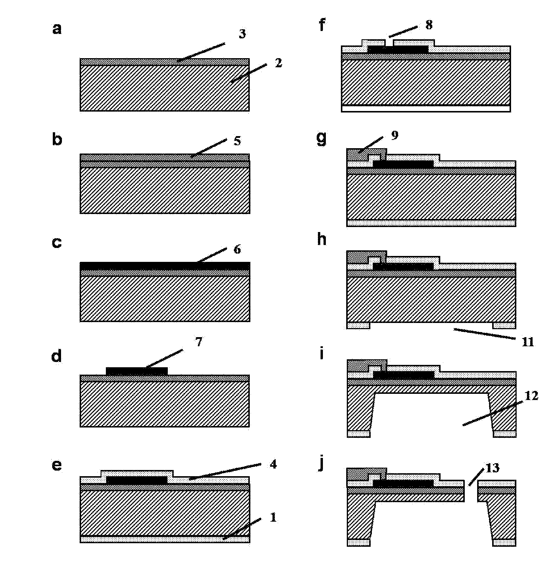
The making and using of various embodiments of the present invention are discussed in detail below with accompanying drawings. It should be appreciated that the present invention provides many applicable inventive concepts that may be embodied in a wide various specific contexts. The sensor is used for quantitative measurement the electromechanical properties and microstructure of the low-dimensional materials.

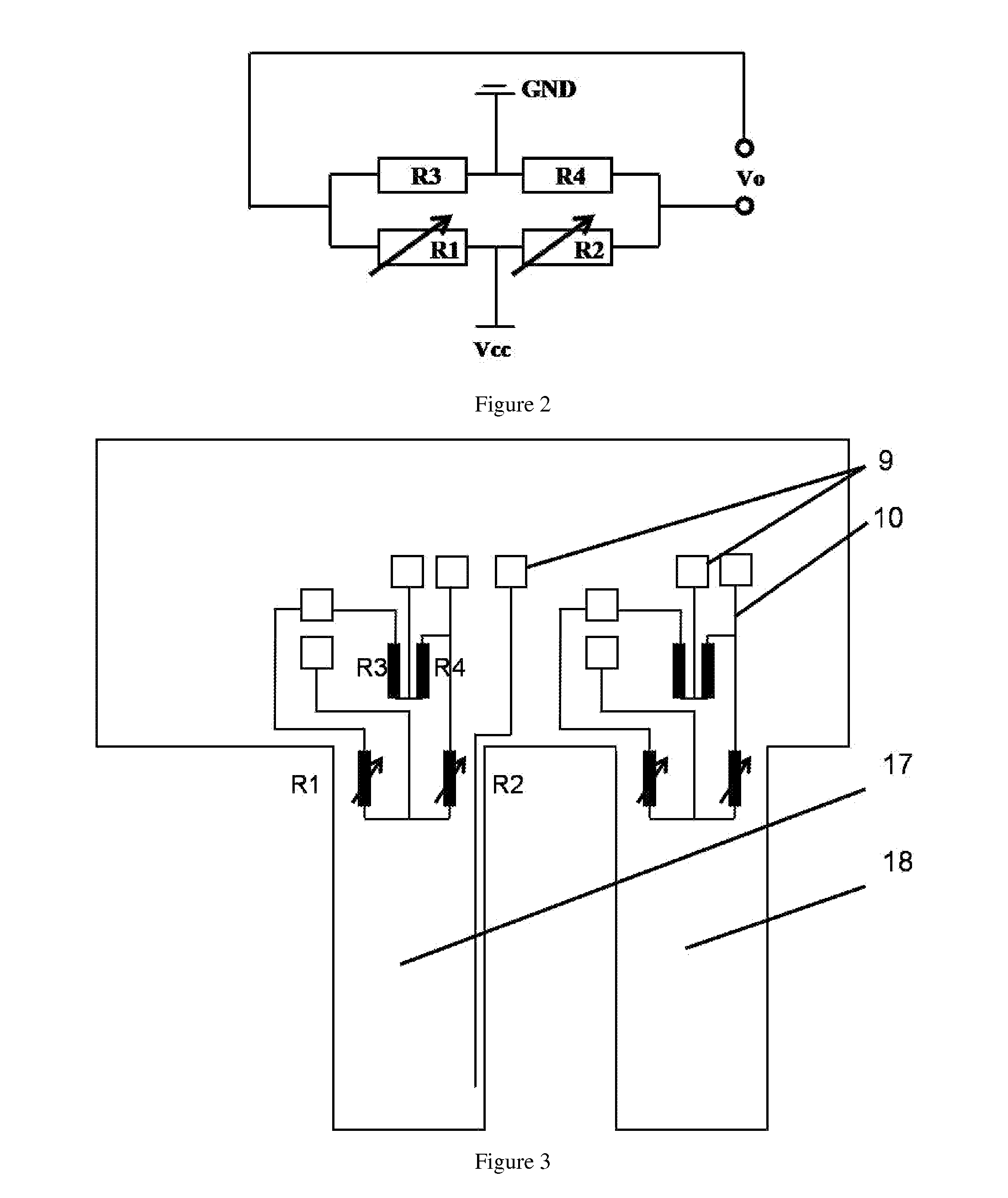
The specific structure of the sensor is shown in FIG. 1-FIG. 6. The sensor for quantitative measurement the electromechanical properties and microstructure of the low-dimensional materials from the bottom up are as follows: a barrier layer (1), silicon substrate (2), epitaxial layer α (3), the epitaxial layer β (5) growth on the epitaxial layers α (3). After doping epitaxial layer β (5), the pressure-sensitive resistor layer (6) is formed. Eight pressure-sensitive resistors (7) are etched and formed on the pressure-sensitive resistor layer (6). There are two variable pressure-...


PUM


Abstract

A sensor for quantitative test electromechanical properties and microstructure of nano-materials and a manufacturing method for the sensor are provided. The sensor comprises a suspended structure, pressure-sensitive resistor cantilevers, support beams, bimetallic strip and other components. When the bimetallic strip produces bending deformation, one of the pressure-sensitive resistor cantilevers is actuated and then stretches the low-dimensional nano-materials which drive the other pressure-sensitive resistor cantilever to bend. Through signal changes are outputted by the Wheatstone bridge, the variable stresses of low-dimensional nano-materials are obtained. Meanwhile, the variable strains of low-dimensional nano-materials are obtained by the horizontal displacements between two cantilevers, so the stress-strain curves of low-dimensional nano-materials are worked out. When the low-dimensional nano-materials are measured in the power state, the voltage-current curves are also obtained. In addition, by the help of high resolution imaging system in the transmission electron microscopy, the mechanical-electrical-microstructure relationship of the nano-materials can be recorded in situ and in atomic lattice resolution.

Description

CROSS-REFERENCE TO RELATED APPLICATIONSThis application claims the priority benefits of China application No. 200910209434.1 filed on Oct. 30, 2009. The contents of China application No. 200910209434.1 are herein incorporated by reference in its entirety.TECHNICAL FIELD OF THE INVENTIONThe present invention relates to a sensor for measuring electro-mechanical properties of low-dimensional nano-materials by in situ high resolution transmission electron microscope (TEM), and a method for producing the sensor. More specifically, the present invention pertains to a TEM sample support or grid that allows the dynamic and real-time measure of the mechanical-electrical-microstructural relationships of individual nanostructure under stress field by in situ TEM at atomic lattice resolution level.BACKGROUND OF THE INVENTIONAs the basic building blocks of the micro- or nano-devices, nano-scale materials carry the information transport, storage and other important functions. The interest in the ...

Claims


Application Information

Patent Timeline
IPC IPC(8): G01Q70/02G01Q70/16
CPCB82Y35/00G01N3/00G01N23/00H01J2237/2062H01J37/20H01J37/26H01J2237/20271G01N2203/0286
Inventor HAN, XIAODONGLIU, PANYUE, YONGHAIZHANG, ZE
Owner BEIJING UNIV OF TECH
Why Eureka
Try Eureka