Fast recovery diode

a fast recovery and diode technology, applied in the field of power electronics, can solve the problems of device failure under much lower supply voltage, high energy ion irradiation, and limited safe operation area of fast recovery diodes, and achieve the effect of fast recovery

Active Publication Date: 2011-05-12
HITACHI ENERGY SWITZERLAND AG
View PDF6 Cites 6 Cited by
  • Summary
  • Abstract
  • Description
  • Claims
  • Application Information

AI Technical Summary

Benefits of technology

[0008]An exemplary embodiment provides a fast recovery diode. The exemplary diode includes an n-doped base layer having a cathode side and an anode side opposite the cathode side. The exemplary diode also includes a p-doped anode layer on the anode side. The anode layer has a doping profile and includes at least two sublayers, which are arranged parallel to the anode side. The at least two sublayers include a first sublayer and a last sublayer. The first sublayer has a first maximum doping concentration, which is between 2*1016 cm−3 and 2*1017 cm−3. The first maximum doping concentration is higher than the maximum doping concentration of any other sublayer of the at least two sublayers. The last sublayer has a last sublayer depth, which is larger than any other sublayer depth. The last sublayer depth being between 90 to 120 μm. The doping profile of the anode layer declines such that a doping concentration in a range of 5*1014 cm−3 and 1*1015 cm−3 is reached between a first depth, which is at least 20 μm, and a second depth, which is at maximum 50 μm. The at least two sublayers are aluminium diffused layers.

Problems solved by technology

Under fast reverse recovery with steep changes of current (high di / dt), the safe operation area (SOA) of fast recovery diodes is seriously limited by dynamic avalanche breakdown.
With increasing recovery di / dt, the dynamic avalanche gets stronger and leads to a device failure under much lower supply voltages as compared to a static breakdown voltage.
However, they just remove the effect by decreasing the amount of free carriers passing through the high electric field region and not the cause, which is the high electric field.
However, this method requires high energy ion irradiation, for which special apparatus are needed.
For wafers with a large diameter, this method requires delicate application, because a homogeneous temperature distribution during annealing, which is required for a controlled p-layer, is difficult to achieve.
There is also a contamination risk during the manufacturing process due to the usage of Palladium.

Method used


Image

  • Fast recovery diode
  • Fast recovery diode
  • Fast recovery diode

Examples


Embodiment Construction

[0020]Exemplary embodiments of the present disclosure provide a fast recovery diode, in which a dynamic avalanche occurs at higher voltages and a static breakdown voltage is increased as compared to known devices.

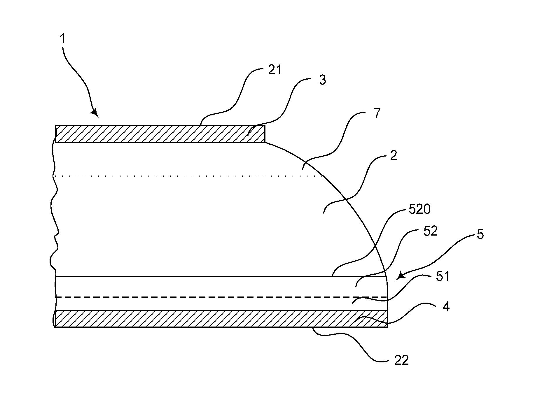
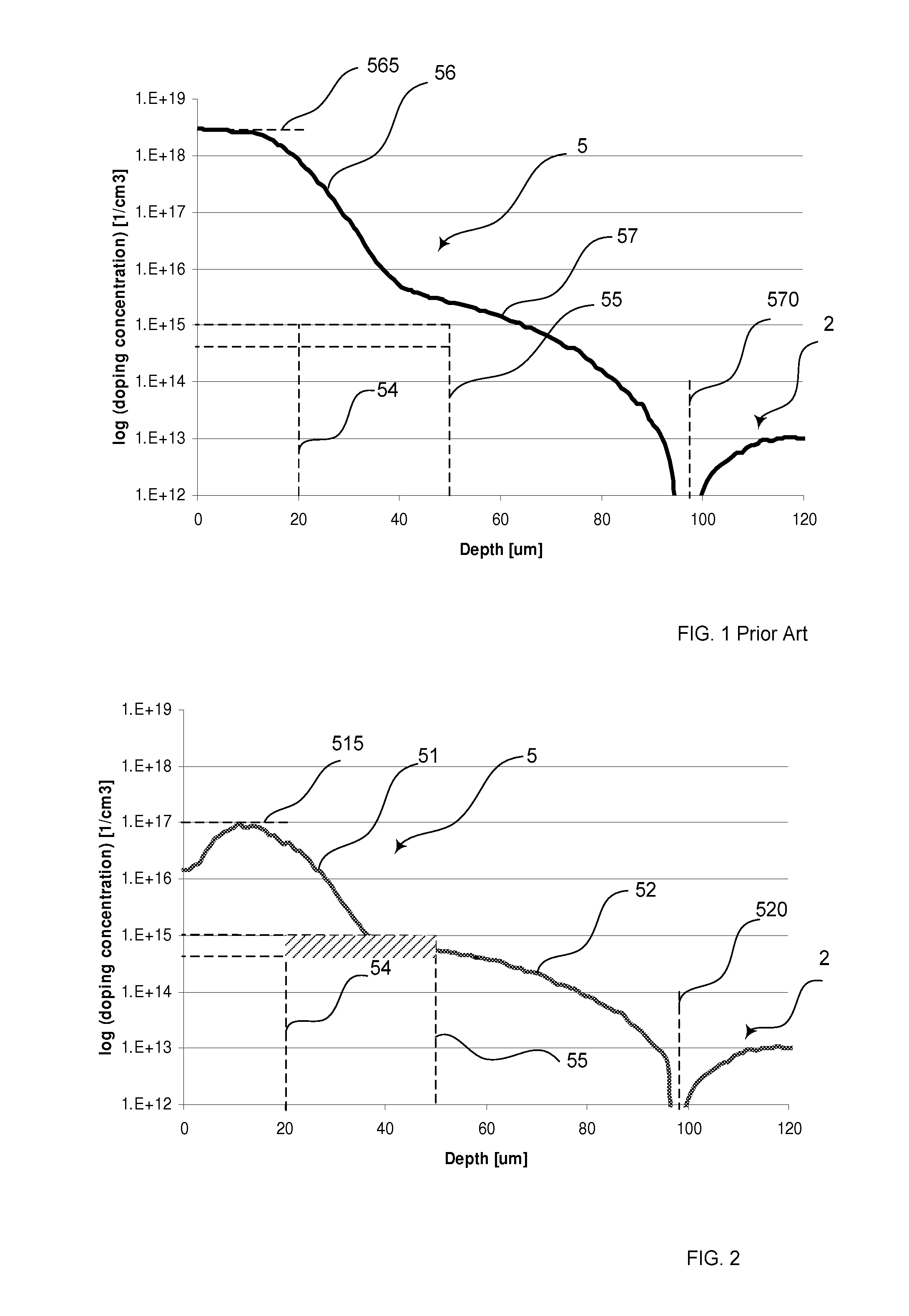
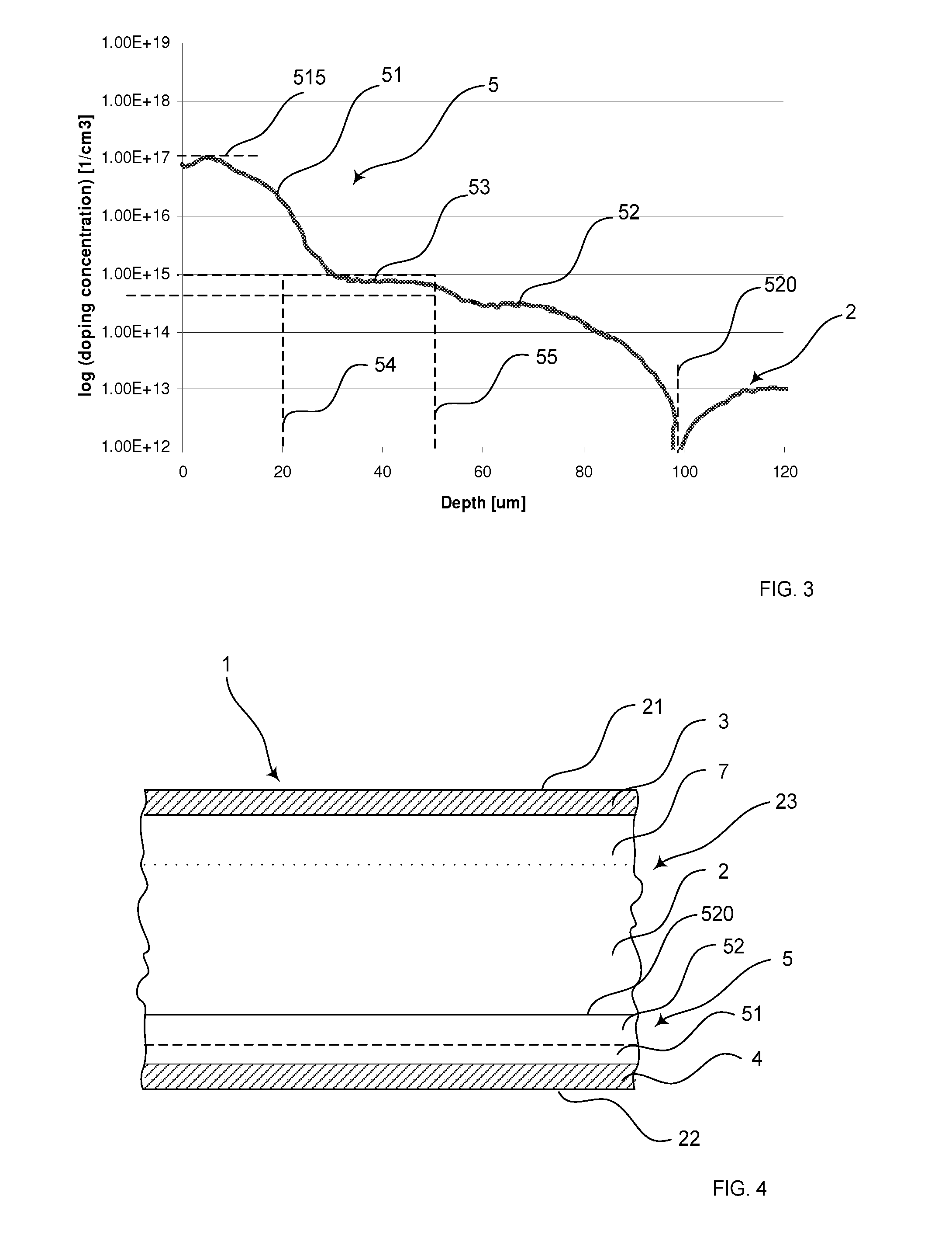
[0021]According to an exemplary embodiment, the fast recovery diode includes an n-doped base layer having a cathode side and an anode side opposite the cathode side. A p-doped anode layer is arranged on the anode side. An anode electrode is arranged on top of the anode layer, i.e. on the side opposite the base layer. The anode electrode can be in the form of a metal layer, for example. The anode layer includes at least two aluminium diffused sublayers, wherein a first sublayer has a first maximum doping concentration, which lies between 2*1016 cm−3 and 2*1017 cm−3 and which first maximum doping concentration is higher than the maximum doping concentration of any other sublayer. The anode layer further includes a last sublayer with a last sublayer depth, which is larger than...


PUM


Abstract

A fast recovery diode includes an n-doped base layer having a cathode side and an anode side opposite the cathode side. A p-doped anode layer is arranged on the anode side. The anode layer has a doping profile and includes at least two sublayers. A first one of the sublayers has a first maximum doping concentration, which is between 2*1016 cm−3 and 2*1017 cm−3 and which is higher than the maximum doping concentration of any other sublayer. A last one of the sublayers has a last sublayer depth, which is larger than any other sublayer depth. The last sublayer depth is between 90 to 120 μm. The doping profile of the anode layer declines such that a doping concentration in a range of 5*1014 cm−3 and 1*1015 cm−3 is reached between a first depth, which is at least 20 μm, and a second depth, which is at maximum 50 μm. Such a profile of the doping concentration is achieved by using aluminium diffused layers as the at least two sublayers.

Description

RELATED APPLICATION[0001]This application claims priority under 35 U.S.C. §119 to European Patent Application No. 09175421.8 filed in Europe on Nov. 9, 2009, the entire content of which is hereby incorporated by reference in its entirety.FIELD[0002]The present disclosure relates to the field of power electronics. More particularly, the present disclosure relates to a fast recovery diode, such as a fast recovery diode for devices with a breakdown voltage above 2.5 kV, and to a method for manufacturing such a fast recovery diode.BACKGROUND INFORMATION[0003]A known diode includes an n-doped base layer having a cathode side and an anode side opposite the cathode side. On the anode side, a p-doped anode layer is arranged, and a metal layer which functions as an anode electrode is arranged on top of the p-doped anode layer. A higher (n+) doped cathode buffer layer is arranged on the cathode side. A metal layer in the form of a cathode electrode is arranged on top of the (n+) doped cathode...

Claims


Application Information

Patent Timeline
Patent Type & Authority Applications(United States)
IPC IPC(8): H01L29/00H01L21/22
CPCH01L29/0661H01L29/32H01L29/8611H01L29/66128H01L29/36
Inventor VOBECKY, JANHEMMANN, KATIDURAN, HAMITRAHIMO, MUNAF
Owner HITACHI ENERGY SWITZERLAND AG
Why Eureka
Try Eureka