

Microstructured sensor for the detection of IR radiation
- Summary
- Abstract
- Description
- Claims
- Application Information
AI Technical Summary
Benefits of technology
Problems solved by technology
Method used
Image

Examples
Embodiment Construction
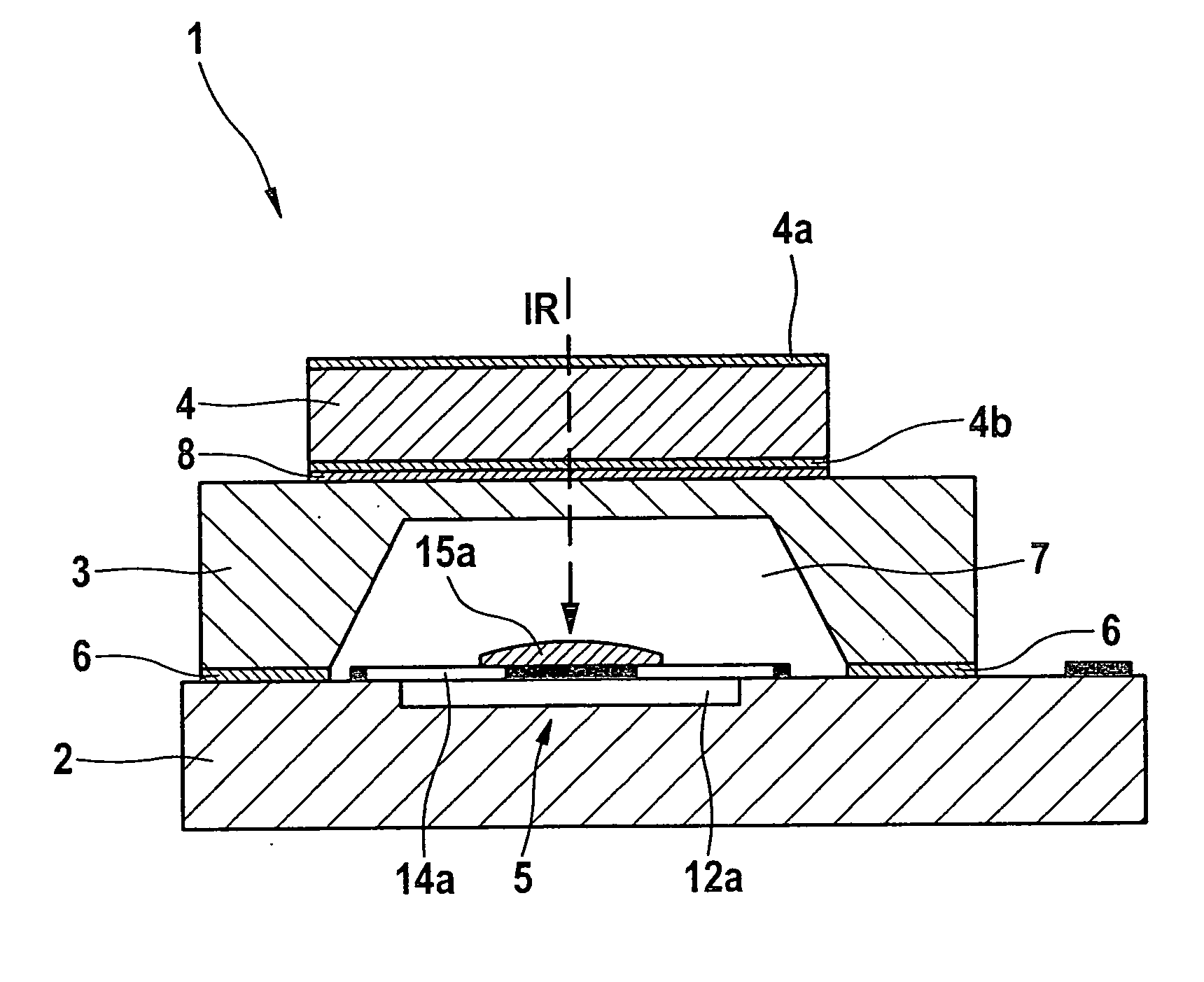
[0021]According to FIG. 1, a sensor 1 has a sensor substrate 2, a cap substrate 3, and a filter substrate 4 or filter chip, which are implemented as a shared stack or chip stack.
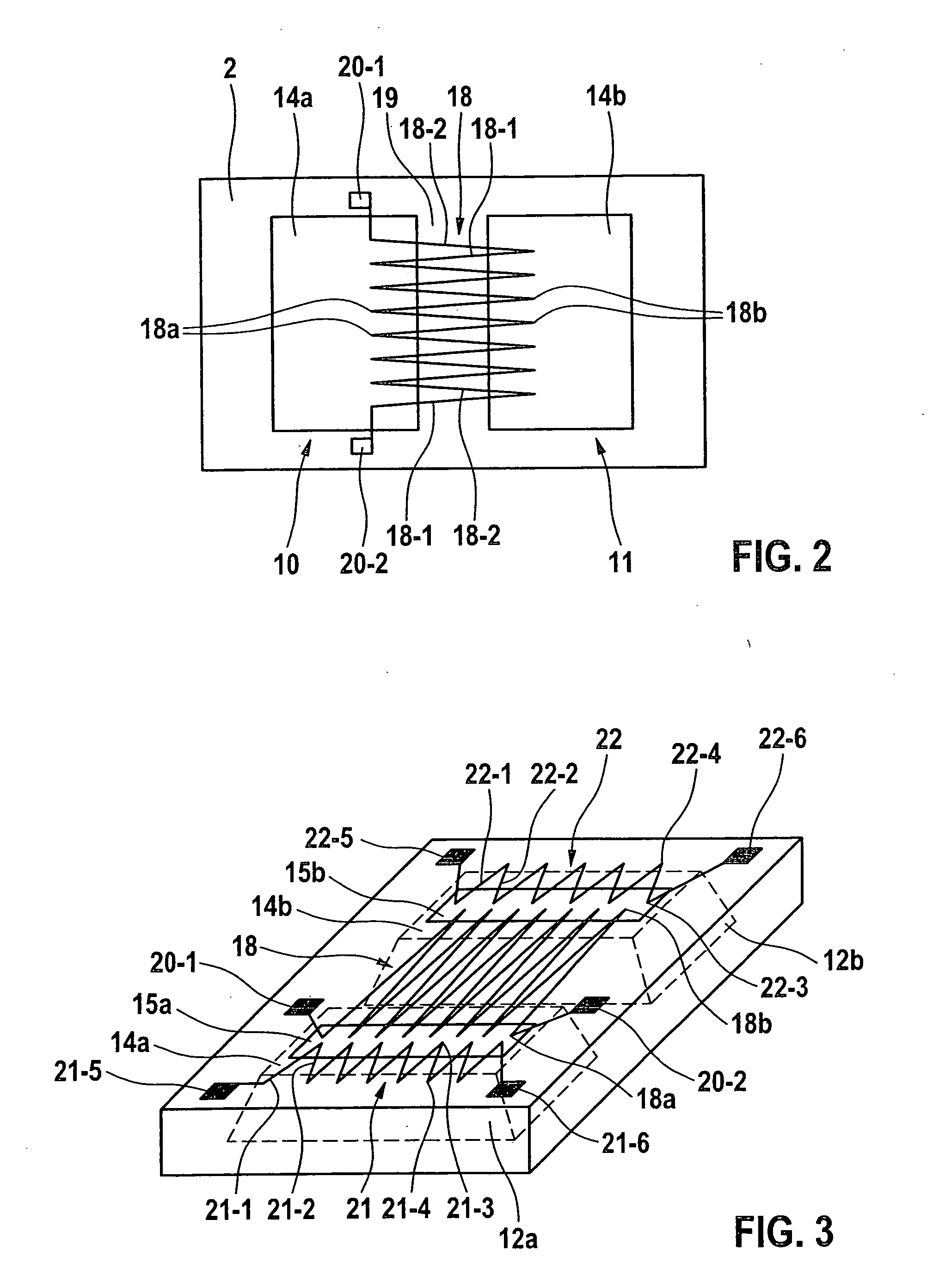
[0022]A sensitive detector structure 5, which has a measuring channel 10 and a reference channel 11, which are shown in greater detail in FIGS. 2 and 3, is implemented on the upper side of sensor substrate 2. Cap substrate 3 is fastened on its lower side using a vacuum-tight seal glass connection 6 on the upper side of sensor substrate 2 outside detector structure 5, so that a cavity 7, which is implemented on the lower side of cap substrate 3, receives detector structure 5 in a vacuum. Filter substrate 4 is fastened on the upper side of cap substrate 3 via an IR-transparent adhesive layer 8. Filter substrate 4 is advantageously structured in such a way that it filters incident IR radiation IR selectively by wavelength and transmits IR radiation of a specified wavelength range in each case to measuring chann...
PUM
 Abstract
Description
Claims
Application Information