Method for creating thermal bonds while minimizing heating of parts

Inactive Publication Date: 2011-05-19
SANTA BARBARA INFRARED
View PDF0 Cites 11 Cited by
  • Summary
  • Abstract
  • Description
  • Claims
  • Application Information

AI Technical Summary

Benefits of technology

[0015]The present invention solves the above-described deficiencies by providing a continuous/semi-continuous large area, thermal and electrical conductive, ambient temperature solder bond for electronic/optical-electronic devices. The method reduces the heating o

Problems solved by technology

Use of high strength bonding materials; e.g. AuSn, can reduce the likelihood of fatigue of the joint and offer excellent heat transfer; however high conventional reflow process temperatures for this material makes it unsuitable for joining temperature sensitive devices or cases where Indium is used to hybridize semiconductor and opto-electronic devices.
Conventional reflow processes using popular bonding materials such as Pb, PbSn, and leadfree solders have higher process temperatures than Indium and subject the Indium to rapid oxidation which can compromise existing bonds resulting in lo

Method used


Image

  • Method for creating thermal bonds while minimizing heating of parts
  • Method for creating thermal bonds while minimizing heating of parts

Examples


Embodiment Construction

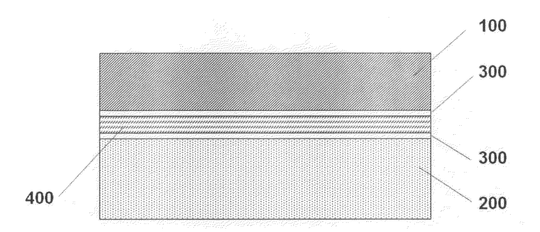
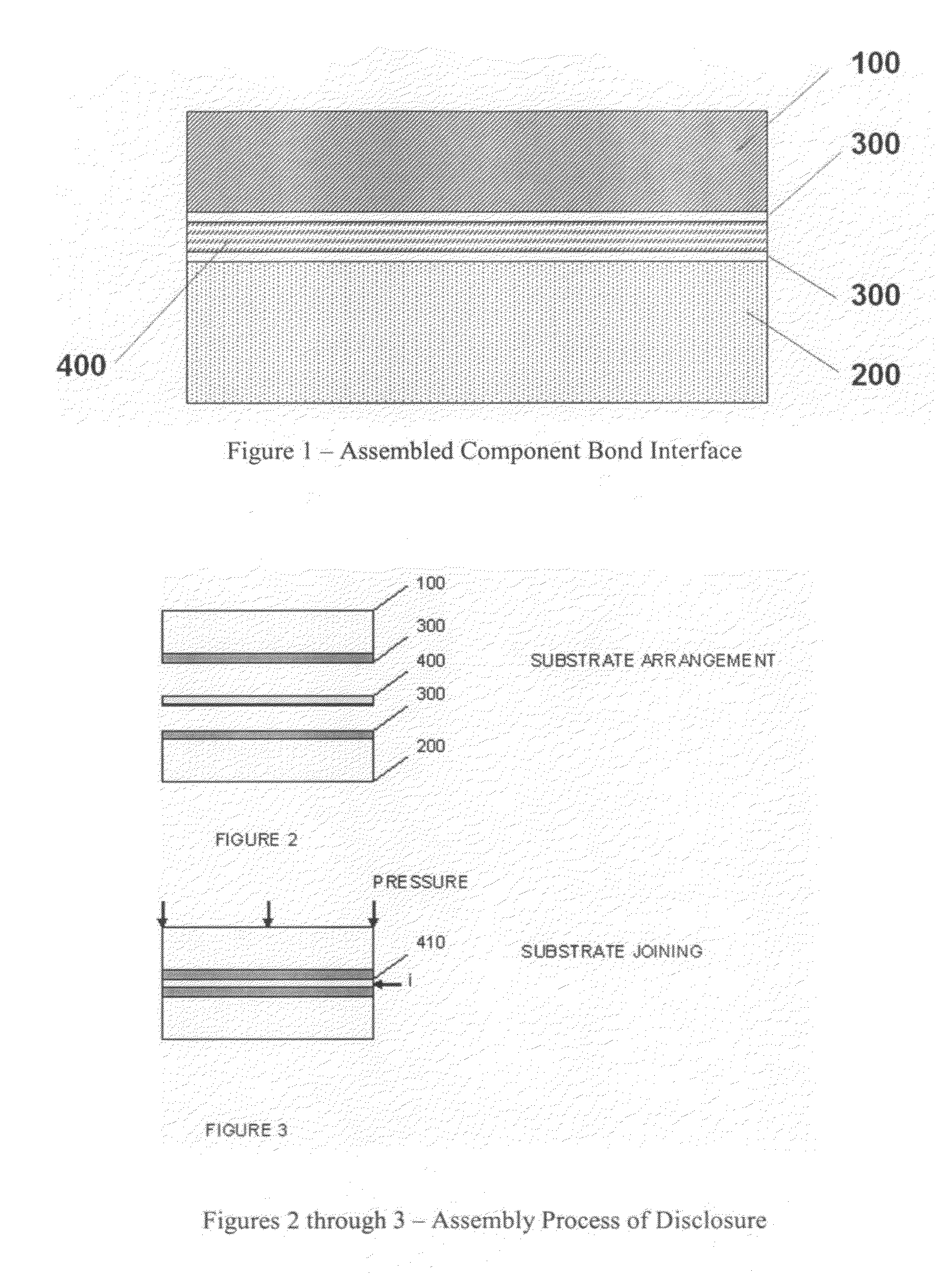
[0019]FIG. 2 shows the two substrates 100 and 200 to be joined separated by a thin multi-layer nano-engineered foil of reactive metal 400. The reactive metal foils 400 are of Ni—Al or Ti—Al class of materials; examples of which are produced by Reactive NanoTechnologies, Hunt Valley, Md. The foils 400 can be made as preforms of various sizes and thickness; and are engineered to produce a non-explosive, nontoxic, single-use, highly controllable exothermic reaction that provides heat selectively to surfaces intimate to the foil 400. The reaction front travels along the foil 400 at speeds between 1- 30 m / sec, raising the local temperature from 25° C. to >1000° C. in 300 are driven by a reduction in chemical bond energy. With a small thermal pulse, atoms diffuse normal to the layering, and Al—Al and Ni—Ni bonds are exchanged for Al—Ni bonds. This local bond exchange produces a large quantity of heat that is conducted down the foil and facilitates more atomic mixing.

[0020]In FIG. 2, both ...


PUM

PropertyMeasurementUnit
Temperatureaaaaaaaaaa
Thicknessaaaaaaaaaa
Structureaaaaaaaaaa

Abstract

A method for making thermally conductive high aspect ratio large area contact between devices while reducing the heating of the devices. The method of the invention includes the use of reactive foils to solder two devices together at room temperature while imparting significantly less temperature rise and resultant residual stress in the bulk devices when compared with conventional reflow solder techniques.

Description

BACKGROUND OF THE INVENTION[0001]1. Field of the Invention[0002]This invention relates generally to the thermally conductive bonding of materials and more particularly thermally conductive bonding of materials that undergo temperature changes where said materials have different coefficients of thermal expansion.[0003]2. Description of the Related Art[0004]In some fields of optical and laser-electronics, and micro-electrical / mechanical devices the component size can be significantly large; e.g. greater than 625 mm2. This is particularly true when dealing with arrayed devices such as imaging sensors, digital liquid crystal displays or attenuators, digital infrared emitters, laser diodes, and deformable mirrors that can be planar, have a curved or a polygonal surface.[0005]Packaging a device typically requires a second component of adequate design and geometry to facilitate a device's operation and provide a means to integrate the device into a product. The device and package component...

Claims


Application Information

Patent Timeline
IPC IPC(8): B23K31/02
CPCB23K2201/40B23K1/0016B23K2101/40
Inventor MATIS, GREGORY P.
Owner SANTA BARBARA INFRARED
Why Eureka
Try Eureka