LED with Improved Injection Efficiency

a technology of injection efficiency and leds, applied in the direction of bulk negative resistance effect devices, electrical equipment, semiconductor devices, etc., can solve the problems of increasing the cost of light sources, increasing the cost of leds, and limiting the power level at which leds opera

Active Publication Date: 2011-05-26
SAMSUNG ELECTRONICS CO LTD
View PDF64 Cites 31 Cited by
  • Summary
  • Abstract
  • Description
  • Claims
  • Application Information

AI Technical Summary

Problems solved by technology

Many high power applications require multiple LEDs to achieve the needed power levels, since individual LEDs are limited to a few watts.
Thus, the cost of many light sources based on LEDs is many times the cost of the individual LEDs.
Heat dissipation places a limit on the power level at which an LED operates.
In addition, the LEDs must be mounted on structures that provide heat dissipation, which, in turn, further increases the cost of the light sources.
In addition, the cost of operation of the LED is also inversely proportional to the conversion efficiency.
However, at high current densities, the efficiency with which holes combine with electrons to produce light decreases.
Hence, as the current is increased through the device, the efficiency decreases and the problems associated with high operating temperatures increase.

Method used


Image

  • LED with Improved Injection Efficiency
  • LED with Improved Injection Efficiency
  • LED with Improved Injection Efficiency

Examples


Embodiment Construction

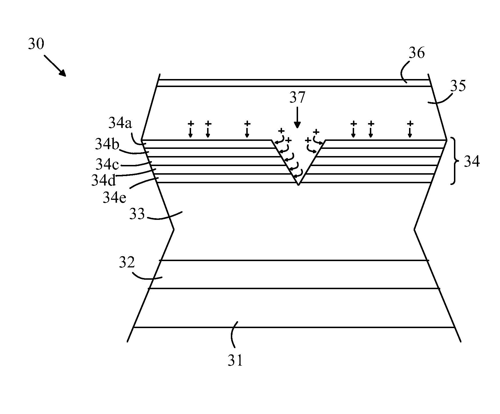
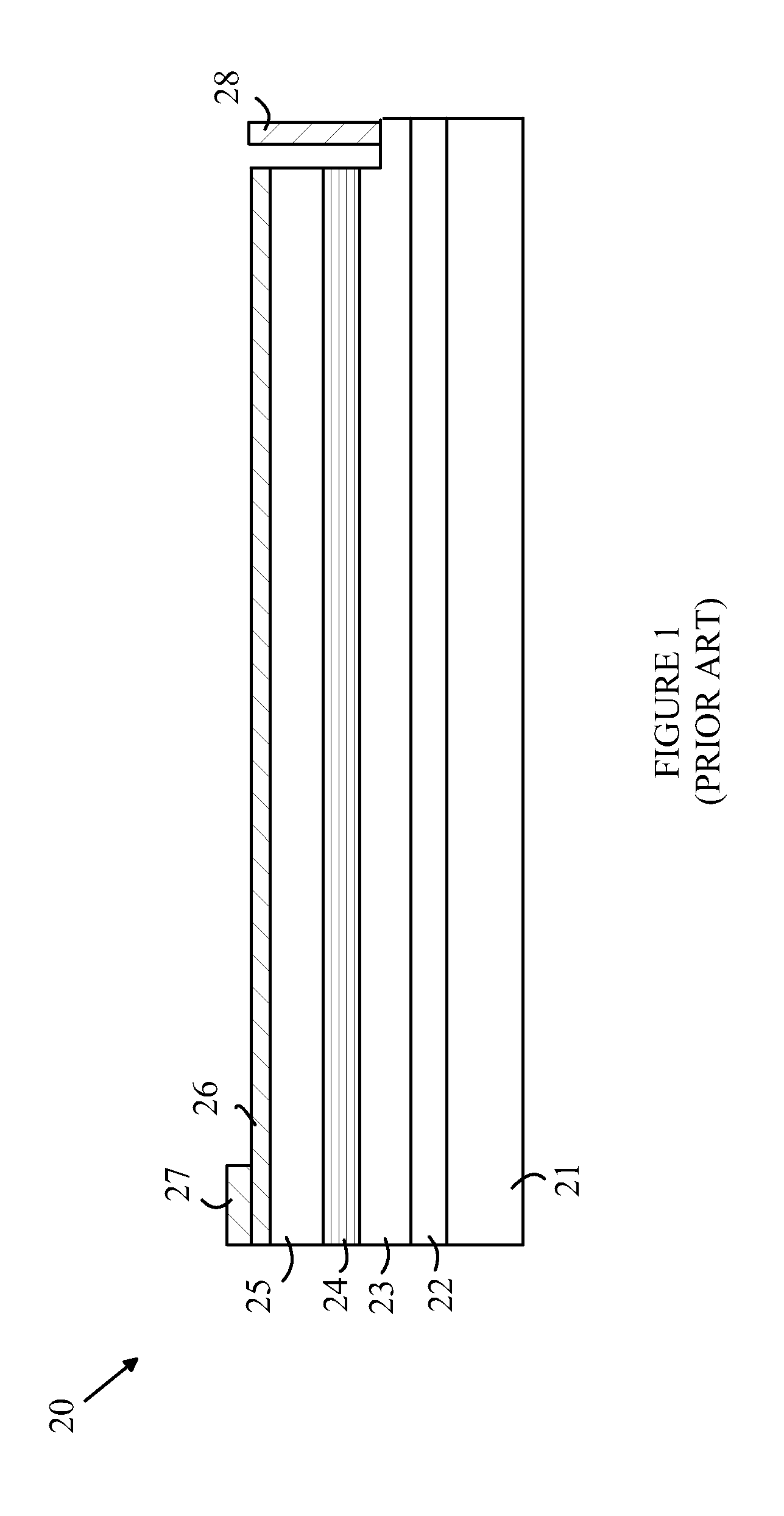
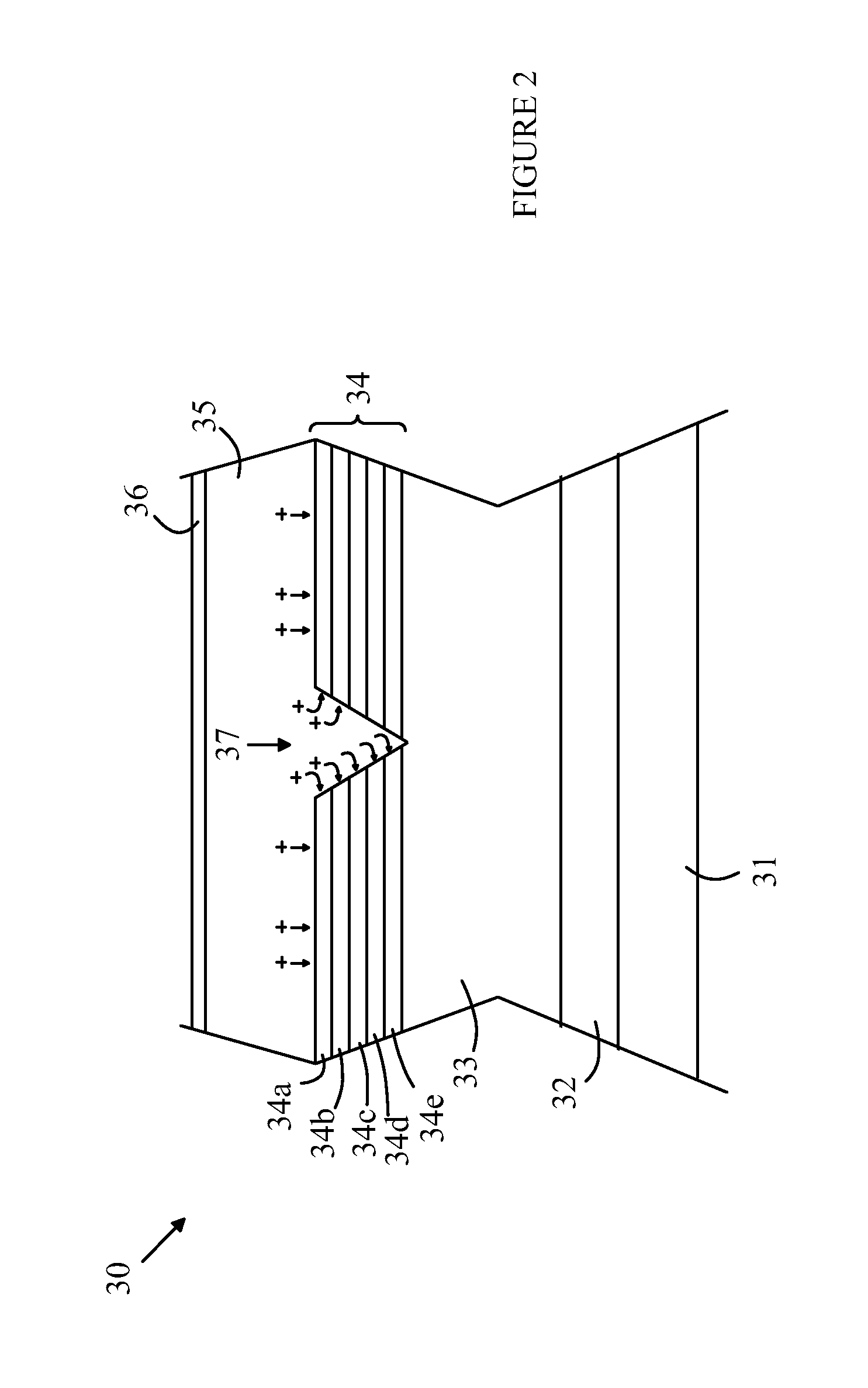
[0019]The manner in which the present invention provides its advantages can be more easily understood with reference to FIG. 1, which is a cross-sectional view of a prior art LED. LED 20 is fabricated on a substrate 21 by depositing a number of layers on the substrate in an epitaxial growth chamber. Typically, a buffer layer 22 is deposited first to compensate for differences in the lattice constants between the lattice constant of the substrate and that of the material system making up the LED layers. For GaN-based LEDs, the substrate is typically sapphire. After buffer layer 22 is deposited, an n-type layer 23 is deposited followed by an active layer 24 and a p-type layer 25. The p-type layer is typically covered by a current spreading layer 26 in GaN LEDs to improve the current distribution through the p-type layer, which has a high resistivity. The device is powered by applying a voltage between contacts 27 and 28.

[0020]The active layer is typically constructed from a number of ...


PUM


Abstract

A light emitting device and method for making the same is disclosed. The light-emitting device includes an active layer sandwiched between a p-type semiconductor layer and an n-type semiconductor layer. The active layer emits light when holes from the p-type semiconductor layer combine with electrons from the n-type semiconductor layer therein. The active layer includes a number of sub-layers and has a plurality of pits in which the side surfaces of a plurality of the sub-layers are in contact with the p-type semiconductor material such that holes from the p-type semiconductor material are injected into those sub-layers through the exposed side surfaces without passing through another sub-layer. The pits can be formed by utilizing dislocations in the n-type semiconductor layer and etching the active layer using an etching atmosphere in the same chamber used to deposit the semiconductor layers without removing the partially fabricated device.

Description

BACKGROUND OF THE INVENTION[0001]Light emitting diodes (LEDs) are an important class of solid-state devices that convert electric energy to light. Improvements in these devices have resulted in their use in light fixtures designed to replace conventional incandescent and fluorescent light sources. The LEDs have significantly longer lifetimes and, in some cases, significantly higher efficiency for converting electric energy to light.[0002]The cost and conversion efficiency of LEDs are important factors in determining the rate at which this new technology will replace conventional light sources and be utilized in high power applications. Many high power applications require multiple LEDs to achieve the needed power levels, since individual LEDs are limited to a few watts. In addition, LEDs generate light in relatively narrow spectral bands. Hence, in applications requiring a light source of a particular color, the light from a number of LEDs with spectral emission in different optical...

Claims


Application Information

Patent Timeline
Patent Type & Authority Applications(United States)
IPC IPC(8): H01L33/30H01L21/20H01L21/302
CPCH01L21/0237H01L21/0243H01L21/02458H01L21/02494H01L21/02505H01L21/0254H01L33/32H01L21/02658H01L33/007H01L33/20H01L33/06H01L33/025H01L33/22H01L21/0262H01L33/0004H01L33/14H01L33/24
Inventor LESTER, STEVENRAMER, JEFFWU, JUNZHANG, LING
Owner SAMSUNG ELECTRONICS CO LTD
Why Eureka
Try Eureka