Semiconductor device and production method thereof

a semiconductor and semiconductor technology, applied in the direction of semiconductor devices, electrical devices, transistors, etc., can solve the problems of silicide layer, variation of operating characteristics, and disadvantageous lowering of the device isolation film surface, so as to prevent the silicide layer from sagging, stabilize the diode current characteristics, and stabilize the emitter width

Active Publication Date: 2011-05-26
RENESAS ELECTRONICS CORP
View PDF4 Cites 3 Cited by
  • Summary
  • Abstract
  • Description
  • Claims
  • Application Information

AI Technical Summary

Benefits of technology

[0015]Since the device isolation film is taller than the substrate at least where it contacts the emitter region, then even if the isolation film is eroded it still will not be lower than the height of the surface of a substrate in the emitter region, as shown in FIGS. 23A and 23B. The device and method according to the invention thus make it possible to prevent the silicide layer from sagging at the end of the emitter region, and control the relationship between the silicide layer and a junction depth to a constant state. This helps to stabilize emitter width and thus to stabilize the diode current characteristics.
[0016]On the other hand, in the MOS transistor region, the gate electrode is formed not only over the diffusion layer but also over the device isolation film. Consequently, it is preferred that the height difference between the substrate and the device isolation film is small adjacent the MOS region so as to maintain gate processing accuracy when lithography is applied during gate forming. In a preferred embodiment, the height of the device isolation film where it contacts the MOS transistor region is less than its height where it contacts the emitter region. This helps to maintain gate processing accuracy.

Problems solved by technology

Consequently, the surface of the device isolation film is disadvantageously lowered relative to the surface of a diffusion layer on a substrate surface at the end of a junction where the diffusion layer touches the device isolation film.
This gives rise to a problem wherein a silicide layer “sags” at the end of a junction where the diffusion layer touches the device isolation film.
However, forming the silicide-free region in that manner may possibly cause variation of operating characteristics.
Further, the end of a diffusion layer may be exposed undesirably because of poor processing dimension accuracy or poor lapping accuracy during the formation of the silicidation mask.
In such a case, a silicide layer will be formed at some locations but not at others, resulting in undesirable variation of operating performance.

Method used


Image

  • Semiconductor device and production method thereof
  • Semiconductor device and production method thereof
  • Semiconductor device and production method thereof

Examples


Embodiment Construction

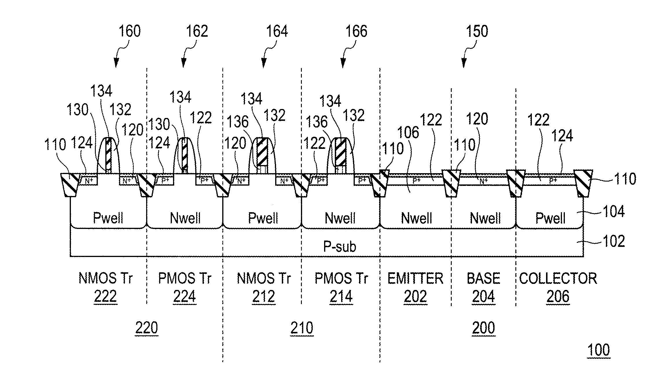
[0041]In FIG. 1, a semiconductor device 100 includes a substrate 102 comprising a MOS transistor region (a core MOS transistor region 220 and an I / O region 210) where a MOS transistor is formed; and a bipolar transistor region 200, where a bipolar transistor 150 is formed, including an emitter region 202, a base region 204, and a collector region 206. In the present embodiment, the substrate 102 can be, for example, a semiconductor substrate such as a silicon substrate or the like. In the following embodiment, the case where a first conductivity type is P-type and a second conductivity type is N-type is shown as an example, but a reverse case is also acceptable.

[0042]Substrate 102 is a P-type substrate. An N well 106 is formed in a region comprising the emitter region 202 and the base region 204 of the bipolar transistor region 200. A p-doped region 122 is formed over the surface of the N well 106 in the emitter region 202. An n-doped region 120 is formed over the surface of the N w...


PUM


Abstract

In a BiCMOS device, a device isolation film separating the bipolar transistor region from the MOS region is taller than the substrate at least where it contacts the bipolar transistor region, and is preferably taller than the same layer where it contacts the MOS transistor region. This makes it possible to maintain the processing accuracy of a MOS transistor while stabilizing the diode current characteristics of the bipolar transistor.

Description

CROSS-REFERENCE TO RELATED APPLICATIONS[0001]The disclosure of Japanese Patent Application No. 2009-264602 filed on Nov. 20, 2009 including the specification, drawings and abstract is hereby incorporated by reference in its entirety.BACKGROUND OF THE INVENTION[0002]1. Field of the Invention[0003]The present invention relates to a BiCMOS semiconductor device and a production method thereof.[0004]2. Description of Related Art[0005]In recent years, a semiconductor device wherein a bipolar transistor, for example, is formed simultaneously on a system LSI including a CMOS comprising a MOSFET (metal oxide semiconductor field-effect transistor) has been developed.[0006]In Japanese Unexamined Patent Publication No. 2008-021671, a blocking layer for blocking the formation of a strain-imparting semiconductor region in a strained channel MOSFET is formed around a base region separated by an element separation layer, with the same process as that for forming the gate electrode section of a CMOS...

Claims


Application Information

Patent Timeline
Patent Type & Authority Applications(United States)
IPC IPC(8): H01L27/102H01L27/092
CPCH01L27/0623H01L21/8249
Inventor MIYAKE, SHINICHITSUNODA, KAZUAKI
Owner RENESAS ELECTRONICS CORP
Why Eureka
Try Eureka